AD9520-1/PCBZ Analog Devices Inc, AD9520-1/PCBZ Datasheet - Page 9
AD9520-1/PCBZ
Manufacturer Part Number
AD9520-1/PCBZ
Description
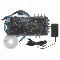
BOARD EVAL FOR AD9520-1
Manufacturer
Analog Devices Inc
Specifications of AD9520-1/PCBZ
Design Resources
Synchronizing Multiple AD9910 1 GSPS Direct Digital Synthesizers (CN0121) Phase Coherent FSK Modulator (CN0186)
Main Purpose
Timing, Clock Generator
Embedded
No
Utilized Ic / Part
AD9520-1
Primary Attributes
12 LVPECL/24 CMOS Output Clock Generator with 2.5 GHz VCO
Secondary Attributes
SPI and I2C Compatible Control Port
Silicon Manufacturer
Analog Devices
Application Sub Type
PLL Clock Synthesizer
Kit Application Type
Clock & Timing
Silicon Core Number
AD9520-0, AD9520-2, AD9520-2
Silicon Family Name
AD9520-X
Rohs Compliant
Yes
Lead Free Status / RoHS Status
Lead free / RoHS Compliant


Evaluation Board User Guide
REGISTER W/R BOX
The REGISTER W/R (write/read) box has three buttons and
three check boxes.
The WRITE button transfers the values stored in the evaluation
software to the evaluation board. It blinks red when register
values have changed.
The READ button transfers the values stored in the evaluation
board to the evaluation software.
The UPDATE button issues an I/O update command by writing
0x01 to Register 0x232.
Selecting the All check box transfers all of the registers when
the WRITE button is clicked. When this box is cleared, only the
registers whose value has changed are written.
Selecting the Auto check box adjacent to the WRITE box
forces the evaluation software to write the register changes
to the evaluation board automatically when they occur.
Selecting the Auto check box adjacent to the UPDATE box
forces the evaluation software to issue an I/O update command
whenever registers are written to the AD9520.
SYNC, PD (POWER DOWN), AND RESET BUTTONS
The SYNC, PD, and RESET buttons allow you to control the
SYNC , PD, and RESET pins on the AD9520.
Each button has three options: Strobe, Latch, and Release.
Strobe activates the pin, and then releases it. Latch holds the
pin active until the Release command is issued.
EEPROM CONTROL WINDOW
The EEPROM Control window shown in Figure 12 is accessed
by clicking the EEPROM button near the lower left corner of
the main window.
To store the current register settings of the AD9520 to the
EEPROM, click the Program EEPROM button (see Figure 12).
Check the EEPROM Status Registers section on the right side
of the window to verify that the operation is successful.
Figure 12. EEPROM Control Window
Rev. 0 | Page 9 of 16
To load the values stored in the EEPROM, ensure that the
EEPROM pin is pulled high and reset the AD9520.
The EEPROM pin is pulled high by placing the S4 EEPROM
jumper (located in the lower left corner of the evaluation board)
across the center and right (high) pin.
You can reset the AD9520 by clicking the red RESET button in
the lower left corner of the main window, and selecting
Strobe ResetB.
REFERENCE (R) DIVIDER WINDOW
The R divider window shown in Figure 13 is accessed by clicking
the R DIVIDER box in the main window. It allows you to set
the reference divider. If this box is colored gray, the PLL is off.
To turn the PLL on, click the PLL MODE box at the top of the
main window, and select Norm Op.
This window has a check box for holding the R divider in reset.
When the R divider is held in reset, the PLL loop is opened.
Therefore, this feature is seldom used.
The reference input path also has a reference multiply-by-2
(labeled X2 in the main window) check box that controls the
reference clock doubler. This frequency doubler can be used
to double the phase detector frequency of the PLL, and is
described in detail in the AD9520 data sheet.
Figure 13. Reference Divider Window
UG-076
Related parts for AD9520-1/PCBZ
Image
Part Number
Description
Manufacturer
Datasheet
Request
R

Part Number:
Description:
12/24 Channel Clock Gen 2,0GH
Manufacturer:
Analog Devices Inc
Datasheet:

Part Number:
Description:
12/24 Channel Clock Gen 2,0GH
Manufacturer:
Analog Devices Inc
Datasheet:
Part Number:
Description:
12/24 Channel Clock Gen 2,0GH
Manufacturer:
Analog Devices Inc
Datasheet:
Part Number:
Description:
12/24 Channel Clock Gen 2,0GH
Manufacturer:
Analog Devices Inc
Datasheet:
Part Number:
Description:
12/24 Channel Clock Gen 2,0GH
Manufacturer:
Analog Devices Inc
Datasheet:
Part Number:
Description:
Clock IC With 2.8GHz On-chip VCO
Manufacturer:
Analog Devices Inc
Datasheet:
Part Number:
Description:
Lock IC With 2.8GHz On-chip VCO
Manufacturer:
Analog Devices Inc
Datasheet:
Part Number:
Description:
12/24 Channel Clock Gen 2,5 GHz VCO
Manufacturer:
Analog Devices Inc
Datasheet:
Part Number:
Description:
12/24 Channel Clock Distribution W/ On-C
Manufacturer:
Analog Devices Inc
Datasheet:
Part Number:
Description:
12/24 Channel Clock Gen 2,25GH
Manufacturer:
Analog Devices Inc
Datasheet:
Part Number:
Description:
12/24 Channel Clock Distribution W/ On-C
Manufacturer:
Analog Devices Inc
Datasheet:
Part Number:
Description:
12/24 Channel Clock Distribution W/ On-C
Manufacturer:
Analog Devices Inc
Datasheet:
Part Number:
Description:
Clock IC With 1.6GHz On-chip VCO
Manufacturer:
Analog Devices Inc
Datasheet:
Part Number:
Description:
Clock IC With 1.6GHz On-chip VCO
Manufacturer:
Analog Devices Inc
Datasheet:
Part Number:
Description:
12/24-Output Clock Generator
Manufacturer:
Analog Devices Inc
Datasheet: