AD9520-1/PCBZ Analog Devices Inc, AD9520-1/PCBZ Datasheet - Page 15
AD9520-1/PCBZ
Manufacturer Part Number
AD9520-1/PCBZ
Description
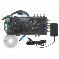
BOARD EVAL FOR AD9520-1
Manufacturer
Analog Devices Inc
Specifications of AD9520-1/PCBZ
Design Resources
Synchronizing Multiple AD9910 1 GSPS Direct Digital Synthesizers (CN0121) Phase Coherent FSK Modulator (CN0186)
Main Purpose
Timing, Clock Generator
Embedded
No
Utilized Ic / Part
AD9520-1
Primary Attributes
12 LVPECL/24 CMOS Output Clock Generator with 2.5 GHz VCO
Secondary Attributes
SPI and I2C Compatible Control Port
Silicon Manufacturer
Analog Devices
Application Sub Type
PLL Clock Synthesizer
Kit Application Type
Clock & Timing
Silicon Core Number
AD9520-0, AD9520-2, AD9520-2
Silicon Family Name
AD9520-X
Rohs Compliant
Yes
Lead Free Status / RoHS Status
Lead free / RoHS Compliant


Evaluation Board User Guide
USING THE EVALUATION BOARD TO PROGRAM AN AD9520 ON A CUSTOMER BOARD
This guide shows how to use an AD9520 evaluation board to
program an AD9520 on a customer board via the I
It assumes that the user has access to the I
on the target board, and knows the assigned address of the
target I
1.
2.
3.
4.
5.
Move Jumper S2 to the center and left (I
Move Jumper W1 to the center and left (I
Select the desired I
board using Jumper S5 and Jumper S6. Note that the S5 =
S6 = high setting is reserved for SPI mode. Also, this I
address should not conflict with the I
target AD9520.
Attach a jumper cable from SDIO_SDA pin of Header P1
of the evaluation board to the SDA pin on the target board.
Repeat Step 4 for both the SCLK_SCL pin and GND pin of
the AD9520 evaluation board to the SCL pin and ground
pin of the target board, respectively. On the evaluation
software, select Configure Serial Port from the I/O menu.
This window is shown in Figure 28.
2
C device.
Figure 28. Evaluation Software Serial Port Configuration
2
C address for the AD9520 evaluation
2
2
C pins via a header
C address of the
2
C) pins.
2
C) pins.
2
C interface.
2
C
Rev. 0 | Page 15 of 16
6.
7.
8.
9.
Click Reset Serial Port and then click Detect Current
Configuration. A dialog box appears and acknowledges
the I
I
that it finds. If the target I
one automatically selected, select the I
target AD9520 from the list, and click OK.
From the View menu on the menu bar (see Figure 24), and
select Debug. Click the I2C Debug button. The window
shown in Figure 29 appears.
Enter the I
the AD9520 evaluation board, and click Ping. The user
should see a green ACK message as shown in Figure 29.
Repeat this step for the I
ACK is returned for both addresses, the remote AD9520 is
ready to be programmed.
If the ping test fails, double-check the cabling between the
boards, as well as the I
Ensure that the I
uation board is different from the target AD9520. Also,
disconnect the jumper cable, and make sure that I
is working properly on the AD9520 evaluation board.
Proceed to program the target AD9520 with the desired
settings. When finished, click the EEPROM button on the
main window to access the EEPROM window, and then
click Program EEPROM to write the settings to the
EEPROM.
2
C Address 0x058 and stops at the first valid I
2
C mode and address. The evaluation software starts at
Figure 29. Evaluation Software I
2
C address set by Jumper S5 and Jumper S6 on
2
C address of the AD9520 on the eval-
2
C address of the target AD9520.
2
C address of the target AD9520. If
2
C address is different from the
2
C Debug Window
2
C address of the
2
C address
UG-076
2
C mode
Related parts for AD9520-1/PCBZ
Image
Part Number
Description
Manufacturer
Datasheet
Request
R

Part Number:
Description:
12/24 Channel Clock Gen 2,0GH
Manufacturer:
Analog Devices Inc
Datasheet:

Part Number:
Description:
12/24 Channel Clock Gen 2,0GH
Manufacturer:
Analog Devices Inc
Datasheet:
Part Number:
Description:
12/24 Channel Clock Gen 2,0GH
Manufacturer:
Analog Devices Inc
Datasheet:
Part Number:
Description:
12/24 Channel Clock Gen 2,0GH
Manufacturer:
Analog Devices Inc
Datasheet:
Part Number:
Description:
12/24 Channel Clock Gen 2,0GH
Manufacturer:
Analog Devices Inc
Datasheet:
Part Number:
Description:
Clock IC With 2.8GHz On-chip VCO
Manufacturer:
Analog Devices Inc
Datasheet:
Part Number:
Description:
Lock IC With 2.8GHz On-chip VCO
Manufacturer:
Analog Devices Inc
Datasheet:
Part Number:
Description:
12/24 Channel Clock Gen 2,5 GHz VCO
Manufacturer:
Analog Devices Inc
Datasheet:
Part Number:
Description:
12/24 Channel Clock Distribution W/ On-C
Manufacturer:
Analog Devices Inc
Datasheet:
Part Number:
Description:
12/24 Channel Clock Gen 2,25GH
Manufacturer:
Analog Devices Inc
Datasheet:
Part Number:
Description:
12/24 Channel Clock Distribution W/ On-C
Manufacturer:
Analog Devices Inc
Datasheet:
Part Number:
Description:
12/24 Channel Clock Distribution W/ On-C
Manufacturer:
Analog Devices Inc
Datasheet:
Part Number:
Description:
Clock IC With 1.6GHz On-chip VCO
Manufacturer:
Analog Devices Inc
Datasheet:
Part Number:
Description:
Clock IC With 1.6GHz On-chip VCO
Manufacturer:
Analog Devices Inc
Datasheet:
Part Number:
Description:
12/24-Output Clock Generator
Manufacturer:
Analog Devices Inc
Datasheet: