AD9520-1/PCBZ Analog Devices Inc, AD9520-1/PCBZ Datasheet - Page 8
AD9520-1/PCBZ
Manufacturer Part Number
AD9520-1/PCBZ
Description
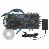
BOARD EVAL FOR AD9520-1
Manufacturer
Analog Devices Inc
Specifications of AD9520-1/PCBZ
Design Resources
Synchronizing Multiple AD9910 1 GSPS Direct Digital Synthesizers (CN0121) Phase Coherent FSK Modulator (CN0186)
Main Purpose
Timing, Clock Generator
Embedded
No
Utilized Ic / Part
AD9520-1
Primary Attributes
12 LVPECL/24 CMOS Output Clock Generator with 2.5 GHz VCO
Secondary Attributes
SPI and I2C Compatible Control Port
Silicon Manufacturer
Analog Devices
Application Sub Type
PLL Clock Synthesizer
Kit Application Type
Clock & Timing
Silicon Core Number
AD9520-0, AD9520-2, AD9520-2
Silicon Family Name
AD9520-X
Rohs Compliant
Yes
Lead Free Status / RoHS Status
Lead free / RoHS Compliant


UG-076
PLL REFERENCE INPUT WINDOW
The Reference Input Control window is shown in Figure 10
and is accessed by clicking either of the triangular buffer
symbols immediately to the right of the REF 1 (MHz) and
REF 2 (MHz) input reference frequency boxes (see Figure 9).
This window is used to enable the PLL reference inputs, which
are powered down by default.
Select Enable REF 1, or Enable REF 2, or both to enable the
appropriate reference input and click OK when finished. If a
differential input is used, select the Use Differential Ref Mode
(Unchecked = Single-Ended Mode) check box. Note that this
mode should not be used simultaneously with Enable REF 1 or
Enable REF 2.
The remaining six check boxes control the reference switchover
modes. If Disable Switchover De-Glitch is activated, the AD9520
maintains the phase relationship between the active input and
PLL output during a reference switchover. Otherwise, the
AD9520 minimizes the phase disturbance at the output
during a reference switchover.
Check Enable XTAL Oscillator if you intend to connect a
crystal to the reference input.
Enable PLL CMOS Ref Input DC Offset forces the dc bias
point of the single-ended reference input to be different from
the switching point, and is useful for preventing an ac-coupled
input from chattering when the reference input is lost.
Figure 10. Reference Input Control Window
Figure 9. Buffer Symbol
Rev. 0 | Page 8 of 16
PLL CONFIGURATION WINDOW
The PLL Configuration window shown in Figure 11 is opened
by clicking the Config PLL button on the main screen. The
window has three sections: SyncB Counter Reset Mode, PLL
Status Registers, and Settings.
The SyncB Counter Reset Mode section indicates whether the
R, A, and B counters are reset when the SYNC pin is activated,
and controls R0x019[7:6]. See the AD9520 data sheet for more
details.
The PLL Status Registers section allows you to see the current
value of the read-only PLL status register, Address 0x01F. This
function is very useful for ensuring that the AD9520 VCO has
finished VCO calibration, and that the PLL is locked.
The Settings section controls the various PLL settings such
as holdover. The AD9520 data sheet describes these functions
in detail.
REFMON, STATUS, AND LD BUTTONS
These three blue buttons (REFMON, STATUS, and LD) allow
you to select which signals appear at the REFMON, STATUS,
and LD pins at Connector P1. Connector P1 is located in the
center of the evaluation board. The pins in the left column of
Connector P1 are ground pins, and the ones in the right
column are signal pins.
There are many useful diagnostic signals available at these
pins. The R divider output is particularly useful. In the example
used in the Quick Start Guide to the AD9520 PLL section, the
80 kHz signal is visible on the STATUS pin to ensure that the
reference inputs and R divider are working properly.
Dynamic signals (such as the R divider output) are primarily
intended for diagnostics. These diagnostic signals may adversely
affect PLL performance in critical applications if left on in
normal operation.
Figure 11. PLL Configuration Window
Evaluation Board User Guide
Related parts for AD9520-1/PCBZ
Image
Part Number
Description
Manufacturer
Datasheet
Request
R

Part Number:
Description:
12/24 Channel Clock Gen 2,0GH
Manufacturer:
Analog Devices Inc
Datasheet:

Part Number:
Description:
12/24 Channel Clock Gen 2,0GH
Manufacturer:
Analog Devices Inc
Datasheet:
Part Number:
Description:
12/24 Channel Clock Gen 2,0GH
Manufacturer:
Analog Devices Inc
Datasheet:
Part Number:
Description:
12/24 Channel Clock Gen 2,0GH
Manufacturer:
Analog Devices Inc
Datasheet:
Part Number:
Description:
12/24 Channel Clock Gen 2,0GH
Manufacturer:
Analog Devices Inc
Datasheet:
Part Number:
Description:
Clock IC With 2.8GHz On-chip VCO
Manufacturer:
Analog Devices Inc
Datasheet:
Part Number:
Description:
Lock IC With 2.8GHz On-chip VCO
Manufacturer:
Analog Devices Inc
Datasheet:
Part Number:
Description:
12/24 Channel Clock Gen 2,5 GHz VCO
Manufacturer:
Analog Devices Inc
Datasheet:
Part Number:
Description:
12/24 Channel Clock Distribution W/ On-C
Manufacturer:
Analog Devices Inc
Datasheet:
Part Number:
Description:
12/24 Channel Clock Gen 2,25GH
Manufacturer:
Analog Devices Inc
Datasheet:
Part Number:
Description:
12/24 Channel Clock Distribution W/ On-C
Manufacturer:
Analog Devices Inc
Datasheet:
Part Number:
Description:
12/24 Channel Clock Distribution W/ On-C
Manufacturer:
Analog Devices Inc
Datasheet:
Part Number:
Description:
Clock IC With 1.6GHz On-chip VCO
Manufacturer:
Analog Devices Inc
Datasheet:
Part Number:
Description:
Clock IC With 1.6GHz On-chip VCO
Manufacturer:
Analog Devices Inc
Datasheet:
Part Number:
Description:
12/24-Output Clock Generator
Manufacturer:
Analog Devices Inc
Datasheet: