AD9520-1/PCBZ Analog Devices Inc, AD9520-1/PCBZ Datasheet - Page 14
AD9520-1/PCBZ
Manufacturer Part Number
AD9520-1/PCBZ
Description
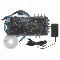
BOARD EVAL FOR AD9520-1
Manufacturer
Analog Devices Inc
Specifications of AD9520-1/PCBZ
Design Resources
Synchronizing Multiple AD9910 1 GSPS Direct Digital Synthesizers (CN0121) Phase Coherent FSK Modulator (CN0186)
Main Purpose
Timing, Clock Generator
Embedded
No
Utilized Ic / Part
AD9520-1
Primary Attributes
12 LVPECL/24 CMOS Output Clock Generator with 2.5 GHz VCO
Secondary Attributes
SPI and I2C Compatible Control Port
Silicon Manufacturer
Analog Devices
Application Sub Type
PLL Clock Synthesizer
Kit Application Type
Clock & Timing
Silicon Core Number
AD9520-0, AD9520-2, AD9520-2
Silicon Family Name
AD9520-X
Rohs Compliant
Yes
Lead Free Status / RoHS Status
Lead free / RoHS Compliant


UG-076
AD9520 PLL LOOP FILTER
The AD9520 PLL requires an external loop filter whose
components are tailored for different applications. The third-
order passive configuration shown in Figure 27 usually offers
the best performance for many applications and is the one
found on the evaluation board.
The default loop filter on the AD9520 evaluation board is
optimized for reference clock cleanup. It has a flat transfer
function with peaking <0.1 dB and loop bandwidths from
0.5 kHz to 10 kHz. In most of these applications, the phase
detector is run at 1 MHz or less.
In the example in the Quick Start Guide to the AD9520 PLL
section, the default loop filter shown in Table 2 results in a PLL
with a loop bandwidth of 2.2 kHz, 80° of phase margin, and
0.05 dB of peaking. The charge pump current for this example
is 1.2 mA.
For clock generation applications in which the reference clock is
relatively low jitter, the high loop bandwidth (BW) loop filter
shown in Table 2 is a better choice. Typical phase detector
frequencies for these applications are 10 MHz to 100 MHz,
and typical loop bandwidths for this loop filter are 50 kHz to
500 kHz, depending on the configuration.
AD9520
CHARGE
PUMP
VCO
Figure 27. PLL Loop Filter
LF
CP
BYPASS
C
BP
= 220nF
C1
R1
C2
R2
C3
Rev. 0 | Page 14 of 16
The user should not consider these recommendations as a
substitute for using ADIsimCLK™ to determine the best loop
filter for a given application. ADIsimCLK is a free program that
can help with the design and exploration of the capabilities and
features of the AD9520, including the design of the PLL loop
filter. The Analog Devices website has a sample ADIsimCLK
file that includes the AD9520 default loop filter titled:
AD9520EvalBoardExample_148p5MHz.clk.
ADIsimCLK Version 1.3 includes specific support for the
AD9520. However, the AD9516, AD9520, and AD9522 share
the same loop dynamics. Therefore, ADIsimCLK Version 1.2
can also be used for modeling the AD9520 loop filter by selecting
the corresponding version of the AD9516. ADIsimCLK is available
at www.analog.com/clocks.
Table 2 shows the correspondence between the components
shown in Figure 27 and those on the evaluation board, as well
as the default values.
Table 2. AD9520 Evaluation Board Default Loop Filter Values
ADIsimCLK
C1
R1
C2
R2
C3
Evaluation
Board Location
C25
R5
C22
R2
C31
Evaluation Board User Guide
Clock Cleanup
(Default)
1500 pF
2.1 kΩ
4.7 μF
3 kΩ
2200 pF
High
Loop BW
62 pF
820 Ω
240 nF
390 Ω
33 pF
Related parts for AD9520-1/PCBZ
Image
Part Number
Description
Manufacturer
Datasheet
Request
R

Part Number:
Description:
12/24 Channel Clock Gen 2,0GH
Manufacturer:
Analog Devices Inc
Datasheet:

Part Number:
Description:
12/24 Channel Clock Gen 2,0GH
Manufacturer:
Analog Devices Inc
Datasheet:
Part Number:
Description:
12/24 Channel Clock Gen 2,0GH
Manufacturer:
Analog Devices Inc
Datasheet:
Part Number:
Description:
12/24 Channel Clock Gen 2,0GH
Manufacturer:
Analog Devices Inc
Datasheet:
Part Number:
Description:
12/24 Channel Clock Gen 2,0GH
Manufacturer:
Analog Devices Inc
Datasheet:
Part Number:
Description:
Clock IC With 2.8GHz On-chip VCO
Manufacturer:
Analog Devices Inc
Datasheet:
Part Number:
Description:
Lock IC With 2.8GHz On-chip VCO
Manufacturer:
Analog Devices Inc
Datasheet:
Part Number:
Description:
12/24 Channel Clock Gen 2,5 GHz VCO
Manufacturer:
Analog Devices Inc
Datasheet:
Part Number:
Description:
12/24 Channel Clock Distribution W/ On-C
Manufacturer:
Analog Devices Inc
Datasheet:
Part Number:
Description:
12/24 Channel Clock Gen 2,25GH
Manufacturer:
Analog Devices Inc
Datasheet:
Part Number:
Description:
12/24 Channel Clock Distribution W/ On-C
Manufacturer:
Analog Devices Inc
Datasheet:
Part Number:
Description:
12/24 Channel Clock Distribution W/ On-C
Manufacturer:
Analog Devices Inc
Datasheet:
Part Number:
Description:
Clock IC With 1.6GHz On-chip VCO
Manufacturer:
Analog Devices Inc
Datasheet:
Part Number:
Description:
Clock IC With 1.6GHz On-chip VCO
Manufacturer:
Analog Devices Inc
Datasheet:
Part Number:
Description:
12/24-Output Clock Generator
Manufacturer:
Analog Devices Inc
Datasheet: