V2DIP1-48 FTDI, Future Technology Devices International Ltd, V2DIP1-48 Datasheet - Page 24
V2DIP1-48
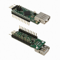
Manufacturer Part Number
V2DIP1-48
Description
MOD MCU-USB HOST CTLR 24-DIP
Manufacturer
FTDI, Future Technology Devices International Ltd
Series
Vinculum-IIr
Datasheet
1.V2DIP1-48.pdf
(25 pages)
Specifications of V2DIP1-48
Main Purpose
Interface, USB 2.0 Host/Controller
Embedded
Yes, ASIC
Utilized Ic / Part
VNC2-48Q
Primary Attributes
Single A-Type Connector, UART / Parallel FIFO / SPI Interfaces
Secondary Attributes
Second USB Port is Available via Pins, Traffic LEDs
Lead Free Status / RoHS Status
Lead free / RoHS Compliant
Other names
768-1057


Document Reference No.: FT_000236
V2DIP1-48 VNC2-48 Development Module Datasheet Version 1.01
Clearance No.: FTDI# 153
`
Appendix B – List of Figures and Tables
List of Figures
Figure 1.1- V2DIP1 48 ................................................................................................................... 1
Figure 3.1 - V2DIP1 48 Module Pin Out (Top View) .......................................................................... 4
Figure 3.2 - V2DIP1 48 Module Pin Out (Bottom View) .................................................................... 5
Figure 3.3 - V2DIP1 48 On-Board Jumper Pin Configuration. .............................................................. 8
Figure 3.4 – Asynchronous FIFO Mode Read and Write Cycle. ........................................................... 13
Figure 3.5 - Synchronous FIFO Mode Read and Write Cycle .............................................................. 14
Figure 5.1 Additional USB Port Configuration .................................................................................. 18
Figure 6.1 V2DIP1 48 Dimensions (Top View) ................................................................................ 19
Figure 6.2 V2DIP1 48 Dimensions (Side View) ............................................................................... 19
Figure 7.1 - Schematic Diagram ................................................................................................... 20
List of Tables
Table 3.1 - Pin Signal Descriptions .................................................................................................. 6
Table 3.2 - V2DIP1 48 Port Selection Jumper Pins ............................................................................. 8
Table 3.3 - Default Interface I/O Pin Configuration ........................................................................... 9
Table 3.4 - Data and Control Bus Signal Mode Options – UART Interface ........................................... 10
Table 3.5 - Data and Control Bus Signal Mode Options – SPI Slave ................................................... 11
Table 3.6 - Data and Control Bus Signal Mode Options – SPI Master ................................................. 12
Table 3.7 - Data and Control Bus Signal Mode Options – Parallel FIFO Interface ................................. 12
Table 3.8 - Asynchronous FIFO Mode Read Cycle Timing .................................................................. 13
Table 3.9 - Data and Control Bus Signal Mode Options – Synchronous FIFO mode .............................. 14
Table 3.10 - Synchronous FIFO Mode Read and Write Cycle Timing ................................................... 15
Table 3.11 - Signal Name and Description – Debugger Interface ....................................................... 16
Copyright © 2010 Future Technology Devices International Limited
23
Related parts for V2DIP1-48
Image
Part Number
Description
Manufacturer
Datasheet
Request
R

Part Number:
Description:
MOD MCU-USB HOST CTLR 24-DIP
Manufacturer:
FTDI, Future Technology Devices International Ltd
Datasheet:

Part Number:
Description:
MOD MCU-USB HOST CTLR 60-DIP
Manufacturer:
FTDI, Future Technology Devices International Ltd
Datasheet:

Part Number:
Description:
IC USB TO SERIAL UART 32-QFN
Manufacturer:
FTDI, Future Technology Devices International Ltd

Part Number:
Description:
IC USB HOST CTLR VINCULUM 48LQFP
Manufacturer:
FTDI, Future Technology Devices International Ltd
Datasheet:

Part Number:
Description:
IC USB HOST VINCULUM-II 32QFN
Manufacturer:
FTDI, Future Technology Devices International Ltd
Datasheet:
Part Number:
Description:
IC USB HOST VINCULUM-II 32LQFN
Manufacturer:
FTDI, Future Technology Devices International Ltd
Datasheet:
Part Number:
Description:
IC USB HOST VINCULUM-II 48QFN
Manufacturer:
FTDI, Future Technology Devices International Ltd
Datasheet:
Part Number:
Description:
IC USB HOST VINCULUM-II 32LQFN
Manufacturer:
FTDI, Future Technology Devices International Ltd
Datasheet:
Part Number:
Description:
IC USB HOST VINCULUM-II 32QFN
Manufacturer:
FTDI, Future Technology Devices International Ltd
Datasheet:
Part Number:
Description:
IC USB HOST VINCULUM-II 48LQFP
Manufacturer:
FTDI, Future Technology Devices International Ltd
Datasheet:
Part Number:
Description:
IC USB HOST VINCULUM-II 48LQFP
Manufacturer:
FTDI, Future Technology Devices International Ltd
Datasheet:
Part Number:
Description:
IC USB HOST VINCULUM-II 48QFN
Manufacturer:
FTDI, Future Technology Devices International Ltd
Datasheet:
Part Number:
Description:
IC USB HOST CTLR VINCULUM 64QFN
Manufacturer:
FTDI, Future Technology Devices International Ltd
Datasheet:

Part Number:
Description:
IC USB HOST CTLR VINCULUM 64LQFP
Manufacturer:
FTDI, Future Technology Devices International Ltd
Datasheet:
Part Number:
Description:
IC USB HOST VINCULUM-II 64LQFP
Manufacturer:
FTDI, Future Technology Devices International Ltd
Datasheet: