ATA6622-EK Atmel, ATA6622-EK Datasheet - Page 4
ATA6622-EK
Manufacturer Part Number
ATA6622-EK
Description
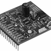
BOARD DEMO LIN SBC FOR ATA6622
Manufacturer
Atmel
Specifications of ATA6622-EK
Main Purpose
Interface, LIN
Embedded
Yes, MCU, 8-Bit
Utilized Ic / Part
ATA6622
Primary Attributes
LIN-SBC (System-Basis-Chip) Transceiver, LIN 2.0, Voltage Regulator, Window Watchdog
Secondary Attributes
4 Power Modes: Pre-Normal, Normal, Sleep, Silent, 20-QFN
Lead Free Status / RoHS Status
Contains lead / RoHS non-compliant


2. Hardware Description
2.1
2.2
2.3
4
Power Supply (VB and GND)
Voltage Regulator (PVCC and VCC)
The Window Watchdog (PTRIG, NTRIG and NRES)
Atmel ATA6621/22/24/26
In the following sections only the normal operating conditions will be described. For further
information concerning one of the mentioned features, refer to the corresponding datasheet.
In order to get the development board running, an external 5.7V to 18V DC power supply is
required between the terminals VB and GND. The input circuit is protected against
inverse-polarity with the protection diode D1, so that there is normally a difference between
the VB and VS level of approximately 0.7V.
The internal 5V/3.3V voltage regulator is capable of driving loads up to 85mA so the SBCs are
able to supply a microcontroller, sensors and/or other ICs. The voltage regulator is protected
against overloads by means of current limitation and overtemperature shutdown. To boost the
maximum load current, an external NPN transistor may be used, with its base being con-
nected to the VCC pin and its emitter connected to PVCC. If this is done, the regulated output
voltage of 5V or 3.3V is available at pin PVCC. For this reason, the pin PVCC and not the pin
VCC is led to the connector available off the board.
But in normal operation, the pins PVCC and VCC have to be connected directly. This is done
by setting jumper J1.
The watchdog anticipates a trigger signal from the microcontroller at the NTRIG input (nega-
tive edge) within a defined time window. The Atmel ATA6621 has an additional PTRIG input,
so it is also possible to trigger the watchdog with a positive edge. If no correct trigger signal is
received, a reset signal will be generated at the NRES output. During Silent or Sleep Mode the
watchdog is switched off to reduce current consumption.
The minimum time for the first watchdog pulse is required after the undervoltage reset at the
NRES pin disappears and is defined as lead time t
The timing basis of the watchdog is provided by the internal oscillator, whose time period t
is adjustable via the external resistor R3 at the pin WD_OSC. For the Atmel ATA6621, the
voltage at this pin is 2.5V, for the Atmel ATA6622/24/26 it is 1.23V (see
through
ings are also different. There is a resistor R3 with a value of 51k
development board, which results in the following timing sequence for the Atmel ATA6621:
Table 1-4 on page
3). Due to these different voltages at the devices, the resulting tim-
d
.
Table 1-2 on page 2
mounted on the
4970B–AUTO–03/11
OSC
Related parts for ATA6622-EK
Image
Part Number
Description
Manufacturer
Datasheet
Request
R

Part Number:
Description:
TXRX LIN BUS REG WATCHDOG 20-QFN
Manufacturer:
Atmel
Datasheet:
Part Number:
Description:
TXRX LIN BUS REG WATCHDOG 20-QFN
Manufacturer:
Atmel
Datasheet:

Part Number:
Description:
LIN Bus Transceiver with 3.3V (5V) Regulator and Watchdog
Manufacturer:
ATMEL Corporation
Datasheet:
Part Number:
Description:
(ATA6622 - ATA6626) LIN Bus Transceiver
Manufacturer:
ATMEL Corporation
Datasheet:

Part Number:
Description:
DEV KIT FOR AVR/AVR32
Manufacturer:
Atmel
Datasheet:
Part Number:
Description:
INTERVAL AND WIPE/WASH WIPER CONTROL IC WITH DELAY
Manufacturer:
ATMEL Corporation
Datasheet:
Part Number:
Description:
Low-Voltage Voice-Switched IC for Hands-Free Operation
Manufacturer:
ATMEL Corporation
Datasheet:
Part Number:
Description:
MONOLITHIC INTEGRATED FEATUREPHONE CIRCUIT
Manufacturer:
ATMEL Corporation
Datasheet:
Part Number:
Description:
AM-FM Receiver IC U4255BM-M
Manufacturer:
ATMEL Corporation
Datasheet:
Part Number:
Description:
Monolithic Integrated Feature Phone Circuit
Manufacturer:
ATMEL Corporation
Datasheet:
Part Number:
Description:
Multistandard Video-IF and Quasi Parallel Sound Processing
Manufacturer:
ATMEL Corporation
Datasheet:
Part Number:
Description:
High-performance EE PLD
Manufacturer:
ATMEL Corporation
Datasheet: