ATA6622-EK Atmel, ATA6622-EK Datasheet
ATA6622-EK
Specifications of ATA6622-EK


Related parts for ATA6622-EK


ATA6622-EK Summary of contents
Page 1
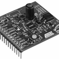
... Introduction The development board for the Atmel ATA6622-EK, ATA6624-EK, ATA6626-EK) is designed to give designers a quick start with the ICs and for prototyping and testing of new LIN designs. The Atmel ATA6621, Atmel ATA6622, Atmel ATA6624 and Atmel ATA6626 are sys- tem basis chips (SBCs) with fully integrated LIN transceiver, window watchdog with adjustable trigger times and low-drop voltage regulator providing 5V/85mA (3 ...
Page 2
... Pre-normal mode (Fail-safe mode) and a 5V (3.3V) DC voltage provided by the internal voltage regulator can be measured between VCC and GND. (The Pre-normal mode is called Fail-safe mode in the datasheets of the devices Atmel ATA6622/24/26). Furthermore, the following voltages or states can be measured at the pins WD_OSC, TEMP, INH, RXD and LIN: Table 1-2 ...
Page 3
... For the quick start it is sufficient to generate a square-wave signal with 75Hz at pin NTRIG or PTRIG for the Atmel ATA6621 or with f = 50Hz at pin NTRIG for the Atmel ATA6622/24/26 (this is recommended only for testing purposes). In order to check that the watchdog is triggered in the expected way, the reset pin NRES can be monitored until a continuous high level is available ...
Page 4
... The timing basis of the watchdog is provided by the internal oscillator, whose time period t is adjustable via the external resistor R3 at the pin WD_OSC. For the Atmel ATA6621, the voltage at this pin is 2.5V, for the Atmel ATA6622/24/ 1.23V (see through ings are also different. There is a resistor R3 with a value of 51k ...
Page 5
... If you want to change the watchdog times mentioned above it is only necessary to change the value of the external resistor R3 (refer to the corresponding datasheet). 4970B–AUTO–03/ 49ms 10ms t = 10.5ms > 3µs trigg ® ATA6622/24/26 the resistor R3 at pin WD_OSC with the same value of 51k = 4ms t = 150ms 20ms > 200ns trigg Atmel ATA6621/22/24/26 Watchdog Reset t = 1.9ms ...
Page 6
... TXD is low, the LIN output transistor is turned on and the bus is in the dominant state. An internal timer prevents the bus line from being driven permanently in the dominant state. If TXD is forced to low longer than t state. This time-out function is disabled in the Atmel ATA6626. 2.4.3 Output Pin (RXD) This pin reports the state of the LIN bus to the microcontroller ...
Page 7
... In the ATA6621 the Reset output is a push-pull state supplied by the VCC voltage. In the Atmel ATA6622/24/26 the Reset output is an open drain output implemented with a sin- gle MOS transistor which is switched on in case of a VCC undervoltage or if the watchdog is not triggered correctly. In order to pull up the NRES output of the Atmel ATA6622/24/26 an external resistor connected to VCC is necessary ...
Page 8
... It is not recommended to exceed this S limit, because the transistor could be damaged as a result of overtemperature higher out- put current is required, additional cooling of the external transistor has to be ensured (see Figure Figure 3-1. Atmel ATA6621/22/24/26 8 3-2, Figure 3-3 and Figure 3-4 on page Boosting the Voltage Regulator 9) ...
Page 9
... 80K/W (No Additional Cooling) max S thJA 150 versus 50K/W (Additional Cooling) max S thJA versus 20K/W (Additional Cooling) max S thJA Atmel ATA6621/22/24/ different coolings or thermal resistances S = 25˚ 85˚ 125˚ ( 25˚ 85˚C = 125˚ ( 25˚ 85˚ 125˚ ( the voltage max ...
Page 10
... Figure 3-5 the Atmel ATA6621. The supply voltage V than V Figure 3-5. Figure 3-6. Atmel ATA6621/22/24/ Figure 3-10 on page 12 show some typical operating characteristics measured at (reverse battery protection). The external circuitry is shown in bat Output Voltage PV versus Battery Voltage V CC ATA6621 with External Boosttransistor MJD31C ...
Page 11
... Figure 3-7. Figure 3-8. 4970B–AUTO–03/11 Atmel ATA6621/22/24/26 Load- transient Response Ch1: I OUT Startup Response Ch1 Ch2 Ch2 ...
Page 12
... Figure 3-9. Figure 3-10. Output Voltage PV Atmel ATA6621/22/24/26 12 Switching from Silent to Normal Mode Ch1: NRES, Ch2: PV versus Temperature at Different Load Currents CC 5,0 5 5,0 4 5 20mA OUT 5 100mA OUT 5 Temperature (° OUT 4970B–AUTO–03/11 ...
Page 13
... GND by replacing resistor. R12 is not mounted. Atmel ATA6621/22/24/26 R10 R10b 0 T1 (ATA6622/24/26) MJD31C TEMP C7 R12 47k 1nF MODE MODE ATA6621/ R3 WD_OSC ATA6622/ 13 ATA6624 51k NRES ATA6626 12 TXD (ATA6622/24/26) R11 47k Revision 2.0 / 2.1 KL_15 D3 LL4148 100nF R1 4.7k R9 PVCC 10k INH LIN C6 220pF ATA6621-EK ATA6622-EK ATA6624-EK ATA6626-EK 13 ...
Page 14
... Figure 4-2. Figure 4-3. Atmel ATA6621/22/24/26 14 Atmel ATA6621/22/24/26 Board Component Placement; Top Side, Top View Atmel ATA6621/22/24/26 Development Board; Top Side, Top View 4970B–AUTO–03/11 ...
Page 15
... Figure 4-4. 4970B–AUTO–03/11 Atmel ATA6621/22/24/26 Atmel ATA6621/22/24/26 Development Board; Bottom Side, Top View (as if PCB Were Transparent) 15 ...
Page 16
... Atmel ATA6621 and the microcontroller ATmega88, a flasher controlled via the LIN bus. The LIN interface of the slave is implemented with the Atmel ATA6624 and the control of the flasher as well as the protocol handling is done by the Atmel ATmega88 microcontroller. In the schematic of this slave node it is obvious that there are almost no other external components needed to fulfill the requirements of this application, other than the development board of the Atmel ATA6621/22/24/26 and the Atmel ATmega88 ...
Page 17
... Furthermore, the flasher produces some glitches, so that there are some capacitors needed in order to block the 12V power supply. Figure 5-2. 4970B–AUTO–03/11 Atmel ATA6621/22/24/26 A Simple Application Using the Development Board for the Atmel ATA6624 (Photograph) 17 ...
Page 18
... Revision History Please note that the following page numbers referred to in this section refer to the specific revision mentioned, not to this document. Revision No. 4970B-AUTO-03/11 Atmel ATA6621/22/24/26 18 History ATA6626 added C Versions added 4970B–AUTO–03/11 ...
Page 19
... Disclaimer: The information in this document is provided in connection with Atmel products. No license, express or implied, by estoppel or otherwise, to any intellec- tual property right is granted by this document or in connection with the sale of Atmel products. EXCEPT AS SET FORTH IN THE ATMEL TERMS AND CONDITIONS OF SALES LOCATED ON THE ATMEL WEBSITE, ATMEL ASSUMES NO LIABILITY WHATSOEVER AND DISCLAIMS ANY EXPRESS, IMPLIED OR STATUTORY WARRANTY RELATING TO ITS PRODUCTS INCLUDING, BUT NOT LIMITED TO, THE IMPLIED WARRANTY OF MERCHANTABILITY, FITNESS FOR A PARTICU- LAR PURPOSE, OR NON-INFRINGEMENT ...