DK-SI-4S100G2N Altera, DK-SI-4S100G2N Datasheet - Page 15
DK-SI-4S100G2N
Manufacturer Part Number
DK-SI-4S100G2N
Description
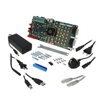
KIT DEV STRATIX IV TRANSCEIVER
Manufacturer
Altera
Series
Stratix® IVr
Datasheet
1.DK-SI-4S100G2N.pdf
(28 pages)
Specifications of DK-SI-4S100G2N
Main Purpose
*
Embedded
*
Utilized Ic / Part
EP4S100G2F40C2ES1
Primary Attributes
*
Secondary Attributes
*
Silicon Manufacturer
Altera
Core Architecture
FPGA
Core Sub-architecture
Stratix
Silicon Core Number
EP4S
Silicon Family Name
Stratix IV GT
Rohs Compliant
Yes
Lead Free Status / RoHS Status
Lead free / RoHS Compliant
Other names
544-2603


Introduction
Test Designs
Table 6–1. Test Design Details
Configuring the FPGA Using Quartus II Programmer
© December 2009 Altera Corporation
signal_integrity_demo1.sof
signal_integrity_demo2.sof
Note to
(1) This is the only transceiver mode available for the corresponding data rate.
Table
File Name
6–1:
1
The kit installs a demonstration application and test designs. The application
provides an easy-to-use interface where you can select various transceiver settings
and observe the result. Before you run the application and test designs, connect the
USB cable to the board and navigate to the Stratix IV GT Transceiver Signal Integrity
Demonstration application as explained in
Development Kit, Stratix IV GT Edition CD-ROM” on page
Altera provides a set of SRAM Object File (.sof) test designs for the evaluation of the
Stratix IV GT device transceiver performance and board features. Before you run the
application, use the Quartus II Programmer to configure the Stratix IV GT device with
one of the .sof files.
source details for each test design.
Early-release kits might not ship with the latest designs and new designs might be
added after kit release. Refer to
on page 5–1
It is sometimes necessary to use the Quartus II Programmer to configure the FPGA
with specific .sof files, such as the designs in
ensure that the Quartus II Programmer and the USB-Blaster driver are installed on the
host computer and the development board is powered up.
Block 2 Channel 0
Block 2 Channel 1
Block 1 Channels 2-5
Block 2 Channel 0
Block 2 Channel 1
Block 0 Channels 6-9
Transceiver Block
and Channel
to access the most current designs and revisions.
Table 6–1
Data Rate
11.3
11.3
10.3125
11.3
11.3
10.3125
(Gbps)
shows file name, data rate, transceiver mode, and clock
Transceiver Signal Integrity Development Kit, Stratix IV GT Edition User Guide
6. Stratix IV GT Transceiver Signal
“Connecting to the Board Update Portal Web Page”
Basic mode with low latency PCS
enabled
Basic mode with low latency PCS
enabled
Basic mode with low latency PCS
enabled
Basic mode with low latency PCS
enabled
Basic mode with low latency PCS
enabled
Basic mode with low latency PCS
enabled
“Installing the Transceiver Signal Integrity
Table
Transceiver Mode
(1)
(1)
(1)
(1)
(1)
(1)
Integrity Demonstration
6–1. Before configuring the FPGA,
3–1.
Y4 (706.25 MHz)
Y4 (706.25 MHz)
Y3 (644.53 MHz)
Y4 (706.25 MHz)
Y4 (706.25 MHz)
Y3 (644.53 MHz)
Clock Source
Related parts for DK-SI-4S100G2N
Image
Part Number
Description
Manufacturer
Datasheet
Request
R

Part Number:
Description:
KIT DEV STRATIX IV 4SGX230N/C2
Manufacturer:
Altera
Datasheet:

Part Number:
Description:
SI KIT W/SII GX EP2SGX90N
Manufacturer:
Altera
Datasheet:

Part Number:
Description:
KIT DEV STRATIX V FPGA 5SGXEA7
Manufacturer:
Altera
Datasheet:

Part Number:
Description:
Programmable Logic IC Development Tools FPGA Starter Kit For Stratix V 5SGXEA7
Manufacturer:
Altera Corporation
Part Number:
Description:
Programmable Logic IC Development Tools FPGA Starter Kit For Stratix V 5SGTMC7
Manufacturer:
Altera Corporation
Part Number:
Description:
Programmable Logic IC Development Tools FPGA Starter Kit For Stratix V 5SGTMC7 ES
Manufacturer:
Altera Corporation

Part Number:
Description:
CYCLONE II STARTER KIT EP2C20N
Manufacturer:
Altera
Datasheet:
Part Number:
Description:
CPLD, EP610 Family, ECMOS Process, 300 Gates, 16 Macro Cells, 16 Reg., 16 User I/Os, 5V Supply, 35 Speed Grade, 24DIP
Manufacturer:
Altera Corporation
Datasheet:
Part Number:
Description:
CPLD, EP610 Family, ECMOS Process, 300 Gates, 16 Macro Cells, 16 Reg., 16 User I/Os, 5V Supply, 15 Speed Grade, 24DIP
Manufacturer:
Altera Corporation
Datasheet:
Part Number:
Description:
Manufacturer:
Altera Corporation
Datasheet:
Part Number:
Description:
CPLD, EP610 Family, ECMOS Process, 300 Gates, 16 Macro Cells, 16 Reg., 16 User I/Os, 5V Supply, 30 Speed Grade, 24DIP
Manufacturer:
Altera Corporation
Datasheet:
Part Number:
Description:
High-performance, low-power erasable programmable logic devices with 8 macrocells, 10ns
Manufacturer:
Altera Corporation
Datasheet:
Part Number:
Description:
High-performance, low-power erasable programmable logic devices with 8 macrocells, 7ns
Manufacturer:
Altera Corporation
Datasheet: