SI2401FS10-EVB Silicon Laboratories Inc, SI2401FS10-EVB Datasheet - Page 7
SI2401FS10-EVB
Manufacturer Part Number
SI2401FS10-EVB
Description
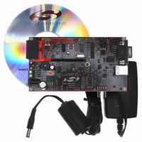
BOARD EVAL SI2401 UART INTERFACE
Manufacturer
Silicon Laboratories Inc
Series
ISOmodem®r
Datasheet
1.SI2401FS10-EVB.pdf
(32 pages)
Specifications of SI2401FS10-EVB
Main Purpose
Telecom, Modem
Embedded
No
Utilized Ic / Part
SI2401
Primary Attributes
Dual RJ-11 Connection to Phone Line, Audio Connector
Secondary Attributes
RS-232, TTL Serial & USB Interfaces
Processor To Be Evaluated
Si2401
Interface Type
RS-232, USB
Lead Free Status / RoHS Status
Contains lead / RoHS non-compliant
Lead Free Status / RoHS Status
Lead free / RoHS Compliant, Contains lead / RoHS non-compliant
Other names
336-1167


3.1.9. Audio Output
Audio output is provided from the Si2401 on the pin,
AOUT. This signal allows the user to monitor call
progress signals, such as dial tone, DTMF dialing, ring,
busy signals, and modem negotiation. Control of this
signal is provided by AT commands and register
settings described in the introduction. The AOUT signal
can be connected to an amplifier, such as the LM386
(the default stuffing option on the Si2401FS10-EVB), for
high-quality output. AOUT can also be connected to a
summing amplifier or multiplexer in an embedded
application as part of an integrated audio system.
3.1.10. Amplifier (LM386)
The audio amplifier circuit consists of U10 (LM386),
C20, R3, R4, C21, C22, C23, R5, C24, and an optional
loudspeaker, LS1. The LM386 has an internally-set
voltage gain of 20. R3 and R4 provide a voltage divider
to reduce the AOUT signal to prevent overdriving the
LM386. C20 provides dc blocking for the input signal
and forms a high-pass filter with R3+R4, while R4 and
C21 form a low-pass filter. These four components limit
the bandwidth of the AOUT signal. C22 provides high-
frequency power supply bypassing for the LM386 and
should be connected to a hard ground and located very
close to the amplifier’s power supply and ground pins.
C23 and R5 form a compensation circuit to prevent
oscillation of the high-current PNP transistor in the
LM386 output stage on negative signal peaks. These
oscillations can occur between 2–5 MHz and can pose
a radiation compliance problem if C23 and R5 are
omitted. C24 provides dc blocking for the output of the
LM386, which is biased at approximately 2.5 V (V
and forms a high-pass filter with the impedance of the
loudspeaker (LS1). The output from the LM386 amplifier
circuit is available on the RCA jack, J2 (not installed).
Install jumper JP13 to enable the onboard speaker, LS1.
3.2. Modem Module Operation
The Si2401FS10-EVB daughter card is a complete
modem solution perfectly suited for use in an embedded
system. The daughter card requires a 3.3 V supply
capable of providing at least 35 mA and communicates
CC
/2),
Rev. 1.1
with the system via LVCMOS/TTL-compatible digital
signals on JP1. The RJ-11 jack (TIP and RING) is
connected via JP2. Be sure to provide the proper
power-on reset pulse to the daughter card if it is used in
the standalone mode.
3.2.1. Reset Requirements
The Si2401 ISOmodem daughter card must be properly
reset at powerup. The reset pin (pin 8) of the Si2401,
(JP1, pin 13), must be held low for at least 5.0 ms after
power is applied and stabilized and returned high with a
rise time less than 100 ns to ensure that the device is
properly reset.
3.2.2. Crystal Requirements
Clock accuracy and stability are important in modem
applications. To ensure reliable communication between
modems, the clock must remain within ±100 ppm of the
design value over the life of the modem. The crystal
selected for use in a modem application must have a
frequency tolerance of less than ±100 ppm for the
combination of initial frequency tolerance, drift over the
normal operating temperature range, and five-year
ageing. Other considerations, such as production
variations in PC board capacitance and the tolerance of
loading capacitors, must also be taken into account.
3.2.3. Protection
The Si2401FS10-EVB meets or exceeds all FCC and
international PTT requirements and recommendations
for high-voltage surge and isolation testing without any
modification. The protection/isolation circuitry includes
C1, C2, C8, C9, FB1, FB2, and RV1. The PCB layout is
also a key “component” in the protection circuitry. The
Si2401FS10-EVB provides isolation to 3 kV. Contact
Silicon Laboratories for information about designing to
higher levels of isolation.
4. Design
The following pages contain the schematics, bill of
materials, and layout for the Si2401 including the
daughter card and motherboard.
Si2401FS10-EVB
7
Related parts for SI2401FS10-EVB
Image
Part Number
Description
Manufacturer
Datasheet
Request
R

Part Number:
Description:
IC ISOMODEM SYSTEM-SIDE 16SOIC
Manufacturer:
Silicon Laboratories Inc
Datasheet:

Part Number:
Description:
Telecom Line Management ICs 2400b/s System Side 3rd Gen DAA Tech
Manufacturer:
Silicon Laboratories Inc
Datasheet:


Part Number:
Description:
V.22bis Isomodem With Integrated Global Daa
Manufacturer:
Silicon Laboratories
Datasheet:

Part Number:
Description:
SMD/C°/SINGLE-ENDED OUTPUT SILICON OSCILLATOR
Manufacturer:
Silicon Laboratories Inc
Part Number:
Description:
Manufacturer:
Silicon Laboratories Inc
Datasheet:
Part Number:
Description:
N/A N/A/SI4010 AES KEYFOB DEMO WITH LCD RX
Manufacturer:
Silicon Laboratories Inc
Datasheet:
Part Number:
Description:
N/A N/A/SI4010 SIMPLIFIED KEY FOB DEMO WITH LED RX
Manufacturer:
Silicon Laboratories Inc
Datasheet:
Part Number:
Description:
N/A/-40 TO 85 OC/EZLINK MODULE; F930/4432 HIGH BAND (REV E/B1)
Manufacturer:
Silicon Laboratories Inc
Part Number:
Description:
EZLink Module; F930/4432 Low Band (rev e/B1)
Manufacturer:
Silicon Laboratories Inc
Part Number:
Description:
I°/4460 10 DBM RADIO TEST CARD 434 MHZ
Manufacturer:
Silicon Laboratories Inc
Part Number:
Description:
I°/4461 14 DBM RADIO TEST CARD 868 MHZ
Manufacturer:
Silicon Laboratories Inc
Part Number:
Description:
I°/4463 20 DBM RFSWITCH RADIO TEST CARD 460 MHZ
Manufacturer:
Silicon Laboratories Inc
Part Number:
Description:
I°/4463 20 DBM RADIO TEST CARD 868 MHZ
Manufacturer:
Silicon Laboratories Inc