SI2401FS10-EVB Silicon Laboratories Inc, SI2401FS10-EVB Datasheet - Page 5
SI2401FS10-EVB
Manufacturer Part Number
SI2401FS10-EVB
Description
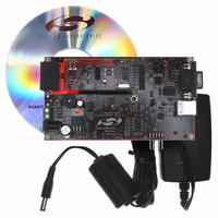
BOARD EVAL SI2401 UART INTERFACE
Manufacturer
Silicon Laboratories Inc
Series
ISOmodem®r
Datasheet
1.SI2401FS10-EVB.pdf
(32 pages)
Specifications of SI2401FS10-EVB
Main Purpose
Telecom, Modem
Embedded
No
Utilized Ic / Part
SI2401
Primary Attributes
Dual RJ-11 Connection to Phone Line, Audio Connector
Secondary Attributes
RS-232, TTL Serial & USB Interfaces
Processor To Be Evaluated
Si2401
Interface Type
RS-232, USB
Lead Free Status / RoHS Status
Contains lead / RoHS non-compliant
Lead Free Status / RoHS Status
Lead free / RoHS Compliant, Contains lead / RoHS non-compliant
Other names
336-1167


3.1.1. Voltage Regulator/Power Supply
The input voltage to either J3 or J4 must be between 7.5
and 13.5 V dc or 7.5 and 13.5 V
motherboard includes a diode bridge (D1–D4) to guard
against a polarity reversal of the dc voltage or to rectify
an ac voltage. The power source must be capable of
continuously supplying at least 100 mA. C50 serves as
a filter cap for an ac input. The voltage regulator, U1,
provides 5 V for the motherboard and the input for
voltage regulator U2, which outputs 3.3 V for use on the
motherboard and to power the daughter card. Si24xxDC
power consumption can be measured by placing a
meter between pins 1 and 2 of JP7. The connection
between JP7 pins 1 and 2 must be made at all times
when power is applied to the evaluation board either
through a jumper block or a low-impedance meter to
avoid damage to the daughter card. Power is supplied
to U2 through D5 from the USB.
3.1.2. Reset Circuitry
The Si2401 requires a reset pulse to remain low for at
least 5.0 ms after the power supply has stabilized during
the powerup sequence or for at least 5.0 ms during a
power-on reset, then go high with a rise time <100 ns.
Most production Si2401 modem chipset applications
require that RESET be controlled by the host processor.
Certain Si2401 operation modes, including Powerdown,
require a hardware reset to recover.
The Si2401FS10-EVB contains two reset options, an
automatic
(default), and a manual reset switch (S1) to permit
resetting
Regardless of the mechanism, a reset causes all
modem settings to revert to factory default values. See
Figure 6 on page 11 and Figure 8 on page 13 for the
reset circuit schematic.
3.1.3. DS1818
The DS1818 is a small, low-cost device that monitors
the voltage on V
V
active-low reset pulse. On power-up, the DS1818 also
outputs an active low reset pulse for 220 ms after V
reaches 90% of the nominal 3.3 V value. The DS1818
outputs a 220 ms reset pulse any time the power supply
voltage exceeds the 3.3 V ±10% window.
3.1.4. Manual Reset
The manual reset switch (S1) performs a power-on
reset. This resets the Si2401 to factory defaults without
turning off power. If S1 is used in conjunction with U6,
pressing S1 activates the reset monitor in the DS1818
and produces a 220 ms active low reset pulse.
D
drops below 3.0 V, the DS1818 provides a 220 ms
of
power-on reset
the
D
and an external reset pushbutton. If
chip
without
device,
removing
PEAK
U3 (DS1818)
ac. The
power.
Rev. 1.1
D
3.1.5. Interface Selection
The serial interface of the Si2401FS10-EVB can be
connected to a computer terminal, embedded system,
or any other Data Terminal Equipment (DTE) via a
standard RS-232 interface, USB interface, or direct TTL
serial interface.
The Si2401 can be tested as a standard data modem by
connecting
computer or other DTE, power supply, and a phone line.
A PC can communicate with the Si2401FS10-EVB
using a standard terminal program, such as HyperTerm
or ProComm.
Jumper settings determine how the Si2401FS10-EVB is
connected to the DTE. Table 3 lists the interface
controlled by each motherboard jumper. See Figure 7
on page 12 and Figure 17 on page 22.
3.1.6. RS-232 Interface
This operation mode uses the standard factory jumper
settings illustrated in Figure 1 on page 3. The Maxim
MAX3237 transceiver interfaces directly with the TTL
levels available at the serial interface of the Si2401 and,
using internal charge pumps, makes these signals
compatible with the RS-232 standard. The RS-232
transceiver on the Si2401FS10-EVB can communicate
at rates between 300 bps and 1 Mbps. This simplifies
the connection to PCs and other Data Terminal
Equipment (DTE). The signals available on the
Si2401FS10-EVB serial interface (DB9 connector) are
listed in Table 4.
Jumper
JP10
JP12
JP11
JP1
JP2
JP3
JP4
JP5
JP6
JP7
JP8
JP9
Table 3. Interface Selection Jumpers
the
Daughter Card Phone Line Connector.
Daughter Card Digital Connector.
Direct Access Header.
Not Used.
USB Enable (RS-232 Disable).
Options.
3.3 V Power for Daughter Card.
Disable both RS-232 and USB.
Not Used.
Not Used.
Not Used.
Enable 27 MHz Clock Option.
Si2401FS10-EVB
Si2401FS10-EVB
Function
to
a
personal
5
Related parts for SI2401FS10-EVB
Image
Part Number
Description
Manufacturer
Datasheet
Request
R

Part Number:
Description:
IC ISOMODEM SYSTEM-SIDE 16SOIC
Manufacturer:
Silicon Laboratories Inc
Datasheet:

Part Number:
Description:
Telecom Line Management ICs 2400b/s System Side 3rd Gen DAA Tech
Manufacturer:
Silicon Laboratories Inc
Datasheet:


Part Number:
Description:
V.22bis Isomodem With Integrated Global Daa
Manufacturer:
Silicon Laboratories
Datasheet:

Part Number:
Description:
SMD/C°/SINGLE-ENDED OUTPUT SILICON OSCILLATOR
Manufacturer:
Silicon Laboratories Inc
Part Number:
Description:
Manufacturer:
Silicon Laboratories Inc
Datasheet:
Part Number:
Description:
N/A N/A/SI4010 AES KEYFOB DEMO WITH LCD RX
Manufacturer:
Silicon Laboratories Inc
Datasheet:
Part Number:
Description:
N/A N/A/SI4010 SIMPLIFIED KEY FOB DEMO WITH LED RX
Manufacturer:
Silicon Laboratories Inc
Datasheet:
Part Number:
Description:
N/A/-40 TO 85 OC/EZLINK MODULE; F930/4432 HIGH BAND (REV E/B1)
Manufacturer:
Silicon Laboratories Inc
Part Number:
Description:
EZLink Module; F930/4432 Low Band (rev e/B1)
Manufacturer:
Silicon Laboratories Inc
Part Number:
Description:
I°/4460 10 DBM RADIO TEST CARD 434 MHZ
Manufacturer:
Silicon Laboratories Inc
Part Number:
Description:
I°/4461 14 DBM RADIO TEST CARD 868 MHZ
Manufacturer:
Silicon Laboratories Inc
Part Number:
Description:
I°/4463 20 DBM RFSWITCH RADIO TEST CARD 460 MHZ
Manufacturer:
Silicon Laboratories Inc
Part Number:
Description:
I°/4463 20 DBM RADIO TEST CARD 868 MHZ
Manufacturer:
Silicon Laboratories Inc