MA180025 Microchip Technology, MA180025 Datasheet - Page 444
MA180025
Manufacturer Part Number
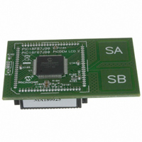
MA180025
Description
MODULE PLUG-IN PIC18F87J90 PIM
Manufacturer
Microchip Technology
Series
PIC®r
Specifications of MA180025
Accessory Type
Plug-In Module (PIM) - PIC18F87J90
Product
Microcontroller Modules
Silicon Manufacturer
Microchip
Core Architecture
PIC
Core Sub-architecture
PIC18
Silicon Core Number
PIC18F
Silicon Family Name
PIC18FxxJxx
Lead Free Status / RoHS Status
Lead free / RoHS Compliant
For Use With/related Products
PICDEM LCD 2 Demonstration Board (DM163030)
For Use With
DM163030 - KIT DEV PICDEM LCD2
Lead Free Status / Rohs Status
Lead free / RoHS Compliant
Available stocks
Company
Part Number
Manufacturer
Quantity
Price
Company:

Part Number:
MA180025
Manufacturer:
Microchip Technology
Quantity:
135
Company:
Part Number:
MA180025
Manufacturer:
MICROCHIP
Quantity:
12 000


PIC18F87J90 FAMILY
DS39933D-page 444
Bus Collision During a Repeated Start
Bus Collision During a Start
Bus Collision During a Stop
Bus Collision During a Stop Condition (Case 2) ....... 253
Bus Collision During Start
Bus Collision for Transmit and Acknowledge............ 249
Capture/Compare/PWM............................................ 415
CLKO and I/O ........................................................... 412
Clock Synchronization .............................................. 235
Clock/Instruction Cycle ............................................... 70
EUSART/AUSART Synchronous Receive
EUSART/AUSART Synchronous Transmission
Example SPI Master Mode (CKE = 0) ...................... 416
Example SPI Master Mode (CKE = 1) ...................... 417
Example SPI Slave Mode (CKE = 0) ........................ 418
Example SPI Slave Mode (CKE = 1) ........................ 419
External Clock ........................................................... 410
Fail-Safe Clock Monitor............................................. 336
First Start Bit Timing ................................................. 243
I
I
I
I
I
I
I
I
I
I
I
I
I
I
LCD Interrupt in Quarter Duty Cycle Drive................ 206
LCD Sleep Entry/Exit When SLPEN = 1
MSSP I
MSSP I
PWM Output ............................................................. 179
Repeated Start Condition.......................................... 244
Reset, Watchdog Timer (WDT), Oscillator Start-up
Send Break Character Sequence ............................. 269
Slave Synchronization .............................................. 217
Slow Rise Time (MCLR Tied to V
SPI Mode (Master Mode) .......................................... 216
SPI Mode (Slave Mode, CKE = 0) ............................ 218
SPI Mode (Slave Mode, CKE = 1) ............................ 218
Synchronous Reception (Master Mode,
Synchronous Transmission............................... 270, 284
Synchronous Transmission
2
2
2
2
2
2
2
2
2
2
2
2
2
2
C Bus Data ............................................................. 421
C Bus Start/Stop Bits.............................................. 420
C Master Mode (7 or 10-Bit Transmission) ............ 246
C Master Mode (7-Bit Reception) ........................... 247
C Slave Mode (10-Bit Reception,
C Slave Mode (10-Bit Reception, SEN = 0) ........... 231
C Slave Mode (10-Bit Reception, SEN = 1) ........... 237
C Slave Mode (10-Bit Transmission)...................... 233
C Slave Mode (7-Bit Reception,
C Slave Mode (7-Bit Reception, SEN = 0) ............. 228
C Slave Mode (7-Bit Reception, SEN = 1) ............. 236
C Slave Mode (7-Bit Transmission)........................ 230
C Slave Mode General Call Address
C Stop Condition Receive or Transmit Mode ......... 248
Condition (Case 2) ............................................ 252
Condition (SCL = 0) .......................................... 251
Condition (Case 1) ............................................ 253
Condition (SDA Only)........................................ 250
(Master/Slave)................................................... 424
(Master/Slave)................................................... 424
SEN = 0, ADMSK = 01001) .............................. 232
SEN = 0, ADMSK = 01011) .............................. 229
Sequence (7 or 10-Bit Addressing Mode)......... 238
or CS1:CS0 = 00............................................... 207
Timer (OST) and Power-up Timer (PWRT) ...... 413
V
SREN)....................................................... 272, 286
(Through TXEN)........................................ 271, 285
DD
2
2
C Bus Data .................................................. 422
C Bus Start/Stop Bits .................................. 422
Rise > T
PWRT
) ............................................. 57
DD
,
Timing Diagrams and Specifications
Top-of-Stack Access........................................................... 67
TSTFSZ ............................................................................ 379
Two-Speed Start-up.................................................. 325, 334
Two-Word Instructions
Time-out Sequence on Power-up (MCLR Not
Time-out Sequence on Power-up (MCLR Not
Time-out Sequence on Power-up (MCLR
Timer Pulse Generation............................................ 170
Timer0 and Timer1 External Clock ........................... 414
Transition for Entry to Idle Mode................................. 50
Transition for Entry to SEC_RUN Mode ..................... 47
Transition for Entry to Sleep Mode ............................. 49
Transition for Two-Speed Start-up
Transition for Wake From Idle to Run Mode............... 50
Transition for Wake From Sleep (HSPLL) .................. 49
Transition From RC_RUN Mode to
Transition From SEC_RUN Mode to
Transition to RC_RUN Mode ...................................... 48
Type-A in 1/2 MUX, 1/2 Bias Drive ........................... 196
Type-A in 1/2 MUX, 1/3 Bias Drive ........................... 198
Type-A in 1/3 MUX, 1/2 Bias Drive ........................... 200
Type-A in 1/3 MUX, 1/3 Bias Drive ........................... 202
Type-A in 1/4 MUX, 1/3 Bias Drive ........................... 204
Type-A/Type-B in Static Drive .................................. 195
Type-B in 1/2 MUX, 1/2 Bias Drive ........................... 197
Type-B in 1/2 MUX, 1/3 Bias Drive ........................... 199
Type-B in 1/3 MUX, 1/2 Bias Drive ........................... 201
Type-B in 1/3 MUX, 1/3 Bias Drive ........................... 203
Type-B in 1/4 MUX, 1/3 Bias Drive ........................... 205
Capture/Compare/PWM Requirements .................... 415
CLKO and I/O Requirements.................................... 412
EUSART/AUSART Synchronous Receive
EUSART/AUSART Synchronous Transmission
Example SPI Mode Requirements (Master Mode,
Example SPI Mode Requirements (Master Mode,
Example SPI Mode Requirements (Slave Mode,
Example SPI Slave Mode Requirements
External Clock Requirements ................................... 410
I
I
Internal RC Accuracy (INTOSC and INTRC)............ 411
MSSP I
MSSP I
PLL Clock ................................................................. 411
Reset, Watchdog Timer, Oscillator Start-up
Timer0 and Timer1 External Clock
Example Cases........................................................... 71
2
2
C Bus Data Requirements (Slave Mode) ............... 421
C Bus Start/Stop Bits Requirements
Tied to V
Tied to V
Tied to V
(INTRC to HSPLL)............................................ 334
PRI_RUN Mode.................................................. 48
PRI_RUN Mode (HSPLL) ................................... 47
Requirements ................................................... 424
Requirements ................................................... 424
CKE = 0) ........................................................... 416
CKE = 1) ........................................................... 417
CKE = 0) ........................................................... 418
(CKE = 1).......................................................... 419
(Slave Mode) .................................................... 420
Timer, Power-up Timer and Brown-out
Reset Requirements......................................... 413
Requirements ................................................... 414
2
2
C Bus Data Requirements .......................... 423
C Bus Start/Stop Bits Requirements........... 422
DD
DD
DD
), Case 1 .......................................... 56
), Case 2 .......................................... 57
, V
DD
2010 Microchip Technology Inc.
Rise Tpwrt) ............................. 56
Related parts for MA180025
Image
Part Number
Description
Manufacturer
Datasheet
Request
R

Part Number:
Description:
Manufacturer:
Microchip Technology Inc.
Datasheet:
Part Number:
Description:
Manufacturer:
Microchip Technology Inc.
Datasheet:
Part Number:
Description:
Manufacturer:
Microchip Technology Inc.
Datasheet:
Part Number:
Description:
Manufacturer:
Microchip Technology Inc.
Datasheet:
Part Number:
Description:
Manufacturer:
Microchip Technology Inc.
Datasheet:
Part Number:
Description:
Manufacturer:
Microchip Technology Inc.
Datasheet:
Part Number:
Description:
Manufacturer:
Microchip Technology Inc.
Datasheet:
Part Number:
Description:
Manufacturer:
Microchip Technology Inc.
Datasheet: