MA180025 Microchip Technology, MA180025 Datasheet - Page 194
MA180025
Manufacturer Part Number
MA180025
Description
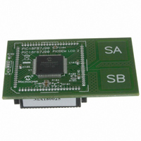
MODULE PLUG-IN PIC18F87J90 PIM
Manufacturer
Microchip Technology
Series
PIC®r
Specifications of MA180025
Accessory Type
Plug-In Module (PIM) - PIC18F87J90
Product
Microcontroller Modules
Silicon Manufacturer
Microchip
Core Architecture
PIC
Core Sub-architecture
PIC18
Silicon Core Number
PIC18F
Silicon Family Name
PIC18FxxJxx
Lead Free Status / RoHS Status
Lead free / RoHS Compliant
For Use With/related Products
PICDEM LCD 2 Demonstration Board (DM163030)
For Use With
DM163030 - KIT DEV PICDEM LCD2
Lead Free Status / Rohs Status
Lead free / RoHS Compliant
Available stocks
Company
Part Number
Manufacturer
Quantity
Price
Company:

Part Number:
MA180025
Manufacturer:
Microchip Technology
Quantity:
135
Company:
Part Number:
MA180025
Manufacturer:
MICROCHIP
Quantity:
12 000


PIC18F87J90 FAMILY
17.7
The rate at which the COM and SEG outputs change is
called the LCD frame frequency. Frame frequency is
set by the LP<3:0> bits (LCDPS<3:0>) and is also
affected by the Multiplex mode being used. The rela-
tionship between the Multiplex mode, LP bits setting
and frame rate is shown in Table 17-4 and Table 17-5.
TABLE 17-4:
TABLE 17-5:
DS39933D-page 194
Multiplex
LP<3:0>
Mode
Static
1/2
1/3
1/4
1
2
3
4
5
6
7
LCD Frame Frequency
Static
Clock Source/(4 x 1 x (LP<3:0> + 1))
Clock Source/(2 x 2 x (LP<3:0> + 1))
Clock Source/(1 x 3 x (LP<3:0> + 1))
Clock Source/(1 x 4 x (LP<3:0> + 1))
125
83
62
50
42
36
31
FRAME FREQUENCY
FORMULAS
APPROXIMATE FRAME
FREQUENCY (IN Hz) FOR LP
PRESCALER SETTINGS
Frame Frequency (Hz)
Multiplex Mode
125
1/2
83
62
50
42
36
31
167
111
1/3
83
67
56
48
42
125
1/4
83
62
50
42
36
31
17.8
LCD waveform generation is based on the principle
that the net AC voltage across the dark pixel should be
maximized and the net AC voltage across the clear
pixel should be minimized. The net DC voltage across
any pixel should be zero.
The COM signal represents the time slice for each
common, while the SEG contains the pixel data. The
pixel signal (COM-SEG) will have no DC component
and it can take only one of the two rms values. The
higher rms value will create a dark pixel and a lower
rms value will create a clear pixel.
As the number of commons increases, the delta
between the two rms values decreases. The delta
represents the maximum contrast that the display can
have.
The LCDs can be driven by two types of waveform:
Type-A and Type-B. In the Type-A waveform, the
phase changes within each common type, whereas in
the Type-B waveform, the phase changes on each
frame boundary. Thus, the Type-A waveform maintains
0 V
waveform takes two frames.
Figure 17-6 through Figure 17-16 provide waveforms
for static, half multiplex, one-third multiplex and quarter
multiplex drives for Type-A and Type-B waveforms.
Note 1: If the power-managed Sleep mode is
DC
over a single frame, whereas the Type-B
2: When the LCD clock source is the system
LCD Waveform Generation
invoked while the LCD Sleep bit (SLPEN)
is set (LCDCON<6> is ‘1’), take care to
execute Sleep only when the V
the pixels is ‘0’.
clock, the LCD module will go to Sleep if
the microcontroller goes into Sleep mode,
regardless of the setting of the SLPEN bit.
Thus, always take care to see that the V
on all pixels is ‘0’ whenever Sleep mode is
invoked.
2010 Microchip Technology Inc.
DC
on all
DC
Related parts for MA180025
Image
Part Number
Description
Manufacturer
Datasheet
Request
R

Part Number:
Description:
Manufacturer:
Microchip Technology Inc.
Datasheet:
Part Number:
Description:
Manufacturer:
Microchip Technology Inc.
Datasheet:
Part Number:
Description:
Manufacturer:
Microchip Technology Inc.
Datasheet:
Part Number:
Description:
Manufacturer:
Microchip Technology Inc.
Datasheet:
Part Number:
Description:
Manufacturer:
Microchip Technology Inc.
Datasheet:
Part Number:
Description:
Manufacturer:
Microchip Technology Inc.
Datasheet:
Part Number:
Description:
Manufacturer:
Microchip Technology Inc.
Datasheet:
Part Number:
Description:
Manufacturer:
Microchip Technology Inc.
Datasheet: