MA180025 Microchip Technology, MA180025 Datasheet - Page 248
MA180025
Manufacturer Part Number
MA180025
Description
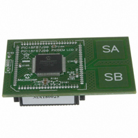
MODULE PLUG-IN PIC18F87J90 PIM
Manufacturer
Microchip Technology
Series
PIC®r
Specifications of MA180025
Accessory Type
Plug-In Module (PIM) - PIC18F87J90
Product
Microcontroller Modules
Silicon Manufacturer
Microchip
Core Architecture
PIC
Core Sub-architecture
PIC18
Silicon Core Number
PIC18F
Silicon Family Name
PIC18FxxJxx
Lead Free Status / RoHS Status
Lead free / RoHS Compliant
For Use With/related Products
PICDEM LCD 2 Demonstration Board (DM163030)
For Use With
DM163030 - KIT DEV PICDEM LCD2
Lead Free Status / Rohs Status
Lead free / RoHS Compliant
Available stocks
Company
Part Number
Manufacturer
Quantity
Price
Company:

Part Number:
MA180025
Manufacturer:
Microchip Technology
Quantity:
135
Company:
Part Number:
MA180025
Manufacturer:
MICROCHIP
Quantity:
12 000


PIC18F87J90 FAMILY
18.4.12
An Acknowledge sequence is enabled by setting the
Acknowledge
(SSPCON2<4>). When this bit is set, the SCL pin is
pulled low and the contents of the Acknowledge data bit
are presented on the SDA pin. If the user wishes to gen-
erate an Acknowledge, then the ACKDT bit should be
cleared. If not, the user should set the ACKDT bit before
starting an Acknowledge sequence. The Baud Rate
Generator then counts for one rollover period (T
and the SCL pin is deasserted (pulled high). When the
SCL pin is sampled high (clock arbitration), the Baud
Rate Generator counts for T
pulled low. Following this, the ACKEN bit is automatically
cleared, the Baud Rate Generator is turned off and the
MSSP module then goes into Idle mode (Figure 18-25).
18.4.12.1
If the user writes the SSPBUF when an Acknowledge
sequence is in progress, then WCOL is set and the
contents of the buffer are unchanged (the write doesn’t
occur).
FIGURE 18-25:
FIGURE 18-26:
DS39933D-page 248
ACKNOWLEDGE SEQUENCE
TIMING
WCOL Status Flag
Note: T
SCL
SDA
Sequence
SSPIF
Note: T
SDA
SCL
Write to SSPCON2,
Falling edge of
Acknowledge sequence starts here,
BRG
ACKNOWLEDGE SEQUENCE WAVEFORM
BRG
STOP CONDITION RECEIVE OR TRANSMIT MODE
9th clock
= one Baud Rate Generator period.
= one Baud Rate Generator period.
ACK
BRG
the end of receive
set PEN
Enable
ACKEN = 1, ACKDT = 0
. The SCL pin is then
SSPIF set at
write to SSPCON2,
bit,
D0
8
T
T
BRG
BRG
SDA asserted low before rising edge of clock
to setup Stop condition
ACKEN
BRG
T
SCL brought high after T
BRG
)
Cleared in
software
T
BRG
P
ACK
SCL = 1 for T
after SDA sampled high. P bit (SSPSTAT<4>) is set.
T
BRG
18.4.13
A Stop bit is asserted on the SDA pin at the end of a
receive/transmit by setting the Stop Sequence Enable
bit,
receive/transmit, the SCL line is held low after the fall-
ing edge of the ninth clock. When the PEN bit is set, the
master will assert the SDA line low. When the SDA line
is sampled low, the Baud Rate Generator is reloaded
and counts down to 0. When the Baud Rate Generator
times out, the SCL pin will be brought high and one
T
SDA pin will be deasserted. When the SDA pin is
sampled high while SCL is high, the P bit
(SSPSTAT<4>) is set. A T
cleared and the SSPIF bit is set (Figure 18-26).
18.4.13.1
If the user writes the SSPBUF when a Stop sequence
is in progress, then the WCOL bit is set and the
contents of the buffer are unchanged (the write doesn’t
occur).
BRG
T
BRG
9
SSPIF set at the end
of Acknowledge sequence
PEN
(Baud Rate Generator rollover count) later, the
PEN bit (SSPCON2<2>) is cleared by
hardware and the SSPIF bit is set
BRG
BRG
, followed by SDA = 1 for T
STOP CONDITION TIMING
(SSPCON2<2>).
ACKEN automatically cleared
WCOL Status Flag
Cleared in
software
2010 Microchip Technology Inc.
BRG
At
BRG
later, the PEN bit is
the
end
of
a
Related parts for MA180025
Image
Part Number
Description
Manufacturer
Datasheet
Request
R

Part Number:
Description:
Manufacturer:
Microchip Technology Inc.
Datasheet:
Part Number:
Description:
Manufacturer:
Microchip Technology Inc.
Datasheet:
Part Number:
Description:
Manufacturer:
Microchip Technology Inc.
Datasheet:
Part Number:
Description:
Manufacturer:
Microchip Technology Inc.
Datasheet:
Part Number:
Description:
Manufacturer:
Microchip Technology Inc.
Datasheet:
Part Number:
Description:
Manufacturer:
Microchip Technology Inc.
Datasheet:
Part Number:
Description:
Manufacturer:
Microchip Technology Inc.
Datasheet:
Part Number:
Description:
Manufacturer:
Microchip Technology Inc.
Datasheet: