MA180025 Microchip Technology, MA180025 Datasheet - Page 188
MA180025
Manufacturer Part Number
MA180025
Description
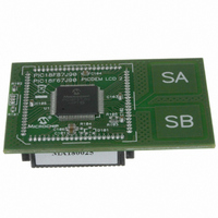
MODULE PLUG-IN PIC18F87J90 PIM
Manufacturer
Microchip Technology
Series
PIC®r
Specifications of MA180025
Accessory Type
Plug-In Module (PIM) - PIC18F87J90
Product
Microcontroller Modules
Silicon Manufacturer
Microchip
Core Architecture
PIC
Core Sub-architecture
PIC18
Silicon Core Number
PIC18F
Silicon Family Name
PIC18FxxJxx
Lead Free Status / RoHS Status
Lead free / RoHS Compliant
For Use With/related Products
PICDEM LCD 2 Demonstration Board (DM163030)
For Use With
DM163030 - KIT DEV PICDEM LCD2
Lead Free Status / Rohs Status
Lead free / RoHS Compliant
Available stocks
Company
Part Number
Manufacturer
Quantity
Price
Company:

Part Number:
MA180025
Manufacturer:
Microchip Technology
Quantity:
135
Company:
Part Number:
MA180025
Manufacturer:
MICROCHIP
Quantity:
12 000


PIC18F87J90 FAMILY
17.2
The LCD driver module generates its internal clock
from 3 possible sources:
• System clock (F
• Timer1 oscillator
• INTRC source
The LCD clock generator uses a configurable
divide-by-32/divide-by-8192 postscaler to produce a
baseline frequency of about 1 kHz nominal, regardless
of the source selected. The clock source selection and
the postscaler configuration are determined by the
Clock Source Select bits, CS<1:0> (LCDCON<3:2>).
An additional programmable prescaler is used to derive
the LCD frame frequency from the 1 kHz baseline. The
prescaler is configured using the LP<3:0> bits
(LCDPS<3:0>) for any one of 16 options, ranging from
1:1 to 1:16.
Proper timing for waveform generation is set by the
LMUX<1:0>
determine which Commons Multiplexing mode is to be
used and divide down the LCD clock source as
required. They also determine the configuration of the
ring counter that is used to switch the LCD commons
on or off.
17.2.1
In addition to the clock source for LCD timing, a
separate 31 kHz nominal clock is required for the LCD
charge pump. This is provided from a distinct branch of
the LCD clock source.
FIGURE 17-2:
DS39933D-page 188
INTOSC 8 MHz Source
System Clock (F
Internal 31 kHz Source
Timer1 Oscillator
LCD Clock Source
LCDCON<3:2>
LCD VOLTAGE REGULATOR
CLOCK SOURCE
bits
OSC
OSC
(LCDCON<1:0>).
/4)
/4)
LCD CLOCK GENERATION
2
LCDCON<1:0>
LCDREG<1:0>
00
01
1x
These
÷256
÷4
÷2
bits
2
00
01
10
11
2
oscillator or the INTRC source, as well as the 8 MHz
prescaler). The charge pump clock source is configured
The charge pump clock can use either the Timer1
INTOSC source (after being divided by 256 by a
using the CKSEL<1:0> bits (LCDREG<1:0>).
17.2.2
When using the system clock as the LCD clock source,
it is assumed that the system clock frequency is a nom-
inal 32 MHz (for a F
Because the prescaler option for the F
selection is fixed at divide-by-8192, system clock
speeds that differ from 32 MHz will produce frame
frequencies and refresh rates different than discussed
in this chapter. The user will need to keep this in mind
when designing the display application.
The Timer1 and INTRC sources can be used as LCD
clock sources when the device is in Sleep mode. To
use the Timer1 oscillator, it is necessary to set the
T1OSCEN bit (T1CON<3>). Selecting either Timer1 or
INTRC as the LCD clock source will not automatically
activate these sources.
Similarly, selecting the INTOSC as the charge pump
clock source will not turn the oscillator on. To use
INTOSC, it must be selected as the system clock
source by using the FOSC2 Configuration bit.
If Timer1 is used as a clock source for the device, either
as an LCD clock source or for any other purpose, LCD
segment 32 become unavailable.
Programmable
LCDPS<3:0>
11
10
01
1:1 to 1:16
Prescaler
4
CLOCK SOURCE
CONSIDERATIONS
÷8192
÷32
or
OSC
2010 Microchip Technology Inc.
Ring Counter
/4 frequency of 8 MHz).
to LCD Charge Pump
÷1, 2, 3, 4
31 kHz Clock
OSC
COM0
COM1
COM2
COM3
/4 clock
Related parts for MA180025
Image
Part Number
Description
Manufacturer
Datasheet
Request
R

Part Number:
Description:
Manufacturer:
Microchip Technology Inc.
Datasheet:
Part Number:
Description:
Manufacturer:
Microchip Technology Inc.
Datasheet:
Part Number:
Description:
Manufacturer:
Microchip Technology Inc.
Datasheet:
Part Number:
Description:
Manufacturer:
Microchip Technology Inc.
Datasheet:
Part Number:
Description:
Manufacturer:
Microchip Technology Inc.
Datasheet:
Part Number:
Description:
Manufacturer:
Microchip Technology Inc.
Datasheet:
Part Number:
Description:
Manufacturer:
Microchip Technology Inc.
Datasheet:
Part Number:
Description:
Manufacturer:
Microchip Technology Inc.
Datasheet: