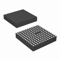
LTM4609IV#PBF Linear Technology, LTM4609IV#PBF Datasheet - Page 20

LTM4609IV#PBF
Manufacturer Part Number
LTM4609IV#PBF
Description
IC BUCK/BOOST SYNC ADJ 4A 141LGA
Manufacturer
Linear Technology
Series
µModuler
Type
Point of Load (POL) Non-Isolatedr
Specifications of LTM4609IV#PBF
Design Resources
LTM4609 Spice Model
Output
0.8 ~ 34 V
Number Of Outputs
1
Power (watts)
136W
Mounting Type
Surface Mount
Voltage - Input
4.5 ~ 36 V
Package / Case
141-LGA
1st Output
0.8 ~ 34 VDC @ 4A
Size / Dimension
0.59" L x 0.59" W x 0.11" H (15mm x 15mm x 2.8mm)
Power (watts) - Rated
136W
Operating Temperature
-40°C ~ 85°C
Efficiency
98%
Dc To Dc Converter Type
Non-Inverting/Inverting/Step Up/Step Down
Pin Count
141
Input Voltage
36V
Output Voltage
0.8 to 34V
Switching Freq
200 TO 400KHz
Output Current
4A
Package Type
LGA
Output Type
Adjustable
Switching Regulator
Yes
Load Regulation
-0.50%
Line Regulation
0.02%/V
Mounting
Surface Mount
Input Voltage (min)
4.5V
Operating Temperature Classification
Industrial
Lead Free Status / RoHS Status
Lead free / RoHS Compliant
3rd Output
-
2nd Output
-
Lead Free Status / Rohs Status
Compliant
Available stocks
Company
Part Number
Manufacturer
Quantity
Price
APPLICATIONS INFORMATION
LTM4609
Layout Checklist/Example
The high integration of LTM4609 makes the PCB board
layout very simple and easy. However, to optimize its electri-
cal and thermal performance, some layout considerations
are still necessary.
• Use large PCB copper areas for high current path, includ-
• Place high frequency input and output ceramic capaci-
• Route SENSE
• Place a dedicated power ground layer underneath the
• To minimize the via conduction loss and reduce module
• Do not put vias directly on pads, unless the vias are
TYPICAL APPLICATIONS
20
ing V
minimize the PCB conduction loss and thermal stress.
tors next to the V
high frequency noise
PC trace spacing. Avoid sense lines passing through
noisy areas, such as switch nodes.
unit.
thermal stress, use multiple vias for interconnection
between the top layer and other power layers
capped.
IN
, R
SENSE
–
and SENSE
, SW1, SW2, PGND and V
IN
, PGND and V
12V TO 36V
+
leads together with minimum
V
IN
1.5k
R1
R3
1k
Figure 16. Buck Mode Operation with 12V to 36V Input
OUT
10μF
50V
×2
pins to minimize
ON/OFF
0.1μF
C3
OUT
. It helps to
PGOOD
RUN
COMP
INTV
PLLFLTR
EXTV
STBYMD
SS
SGND
CC
CC
V
LTM4609
IN
PGND
PLLIN
• Use a separated SGND ground copper area for com-
Figure 15. gives a good example of the recommended
layout.
SENSE
SENSE
SW1
V
PGND
R
ponents connected to signal pins. Connect the SGND
to PGND underneath the unit.
OUT
SENSE
V
SW1
SW2
FCB
C
OUT
V
OUT
FB
+
–
CLOCK SYNC
4.7μH
L1
R
7.15k
Figure 15. Recommended PCB Layout
FB
R2
9mΩ
KELVIN CONNECTIONS TO R
4609 TA02
+ –
+
L1
R
100μF
25V
SENSE
SGND
V
12V
10A
OUT
SW2
V
IN
SENSE
R
SENSE
PGND
C
IN
4609 F15
4609fa


