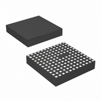
LTM4609IV#PBF Linear Technology, LTM4609IV#PBF Datasheet - Page 15

LTM4609IV#PBF
Manufacturer Part Number
LTM4609IV#PBF
Description
IC BUCK/BOOST SYNC ADJ 4A 141LGA
Manufacturer
Linear Technology
Series
µModuler
Type
Point of Load (POL) Non-Isolatedr
Specifications of LTM4609IV#PBF
Design Resources
LTM4609 Spice Model
Output
0.8 ~ 34 V
Number Of Outputs
1
Power (watts)
136W
Mounting Type
Surface Mount
Voltage - Input
4.5 ~ 36 V
Package / Case
141-LGA
1st Output
0.8 ~ 34 VDC @ 4A
Size / Dimension
0.59" L x 0.59" W x 0.11" H (15mm x 15mm x 2.8mm)
Power (watts) - Rated
136W
Operating Temperature
-40°C ~ 85°C
Efficiency
98%
Dc To Dc Converter Type
Non-Inverting/Inverting/Step Up/Step Down
Pin Count
141
Input Voltage
36V
Output Voltage
0.8 to 34V
Switching Freq
200 TO 400KHz
Output Current
4A
Package Type
LGA
Output Type
Adjustable
Switching Regulator
Yes
Load Regulation
-0.50%
Line Regulation
0.02%/V
Mounting
Surface Mount
Input Voltage (min)
4.5V
Operating Temperature Classification
Industrial
Lead Free Status / RoHS Status
Lead free / RoHS Compliant
3rd Output
-
2nd Output
-
Lead Free Status / Rohs Status
Compliant
Available stocks
Company
Part Number
Manufacturer
Quantity
Price
APPLICATIONS INFORMATION
For the input capacitor, only minimum capacitors are
needed to handle the maximum RMS current, since it
is a continuous input current at boost mode. A 100μF
capacitor is only needed if the input source impedance is
compromised by long inductive leads or traces.
Since the output capacitors at boost mode need to fi lter
the square wave current, more capacitors are expected
to achieve the same output ripples as the buck mode. If
assuming that the ESR dominates the output ripple, the
output ripple is as follows:
If a total low ESR about 5mΩ is chosen for output capaci-
tors, the maximum output ripple of 70mV occurs at the input
voltage of 5V with the peak inductor current at 14A.
An RC snubber is recommended on SW1 to obtain low
switching noise, as shown in Figure 17.
Figure 4. Current Ripple Ratio at Different Inputs for Boost Mode
ΔV
OUT(P-P)
0.8
0.6
0.4
0.2
0
= ESR •I
5
6
INPUT VOLTAGE V
L(MAX)
7
1.5μH
2.5μH
3.3μH
4.7μH
8
9
IN
(V)
10
11
4609 F04
12
Wide Input Mode Operation
If a wide input range is required from 5V to 36V, the module
will work in different operation modes. If input voltage
V
needs to consider the worst case in buck or boost mode
design. Therefore, the maximum output power is limited
to 60W. The sensing resistor is chosen at 8mΩ, the input
capacitor is the same as the buck mode design and the
output capacitor uses the boost mode design. Since the
maximum output ripple normally occurs at boost mode
in the wide input mode design, more inductor ripple cur-
rent, up to 150% of the inductor current, is allowed at
buck mode to meet the ripple design requirement. Thus,
a 3.3μH inductor is chosen at the wide input mode. The
maximum output ripple voltage is still 70mV if the total
ESR is about 5mΩ.
Additionally, the current limit may become very high when
the module runs at buck mode due to the low sensing
resistor used in the wide input mode operation.
Safety Considerations
The LTM4609 modules do not provide isolation from V
V
with a rating twice the maximum input current needs to be
provided to protect each unit from catastrophic failure.
IN
OUT
= 5V to 36V, V
. There is no internal fuse. If required, a slow blow fuse
OUT
= 12V and ƒ = 400kHz, the design
LTM4609
15
IN
4609fa
to


