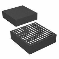
LTM8027IV#PBF Linear Technology, LTM8027IV#PBF Datasheet - Page 15

LTM8027IV#PBF
Manufacturer Part Number
LTM8027IV#PBF
Description
IC BUCK SYNC ADJ 4A 113LGA
Manufacturer
Linear Technology
Series
µModuler
Type
Point of Load (POL) Non-Isolatedr
Datasheet
1.LTM8027MPVPBF.pdf
(22 pages)
Specifications of LTM8027IV#PBF
Design Resources
LTM8027 Spice Model
Output
2.5 ~ 24 V
Number Of Outputs
1
Power (watts)
96W
Mounting Type
Surface Mount
Voltage - Input
4.5 ~ 60 V
Package / Case
113-LGA
1st Output
2.5 ~ 24 VDC @ 4A
Size / Dimension
0.59" L x 0.59" W x 0.17" H (15mm x 15mm x 4.32mm)
Power (watts) - Rated
96W
Operating Temperature
-40°C ~ 125°C
Efficiency
95%
Primary Input Voltage
60V
No. Of Outputs
1
Output Voltage
24V
Output Current
4A
No. Of Pins
113
Operating Temperature Range
-40°C To +125°C
Voltage Regulator Type
Buck DC/DC Converter
Rohs Compliant
Yes
Lead Free Status / RoHS Status
Lead free / RoHS Compliant
3rd Output
-
2nd Output
-
Available stocks
Company
Part Number
Manufacturer
Quantity
Price
APPLICATIONS INFORMATION
Ensure that the grounding and heatsinking are acceptable.
A few rules to keep in mind are:
1. Place the R
2. Place the C
3. Place the C
4. Place the C
5. Connect all of the GND connections to as large a copper
Use vias to connect the GND copper area to the board’s
internal ground planes. Liberally distribute these GND vias
to provide both a good ground connection and thermal
path to the internal planes of the printed circuit board. Pay
attention to the location and density of the thermal vias in
their respective pins.
and GND connection of the LTM8027.
V
ground current flow directly adjacent to or underneath
the LTM8027.
pour or plane area as possible on the top layer. Avoid
breaking the ground connection between the external
components and the LTM8027.
OUT
and GND connection of the LTM8027.
ADJ
IN
OUT
IN
capacitor as close as possible to the V
and R
and C
capacitor as close as possible to the
T
OUT
resistors as close as possible to
capacitors such that their
RUN
SS
R
GND
ADJ
BIAS1
BIAS2
AUX
R
T
SYNC
Figure 3. Suggested Layout
IN
Figure 3. The LTM8027 can benefit from the heat sinking
afforded by vias that connect to internal GND planes at
these locations, due to their proximity to internal power
handling components. The optimum number of thermal
vias depends upon the printed circuit board design. For
example, a board might use very small via holes. It should
employ more thermal vias than a board that uses larger
holes.
Thermal Considerations
The LTM8027 output current may need to be derated if it
is required to operate in a high ambient temperature or
deliver a large amount of continuous power. The amount
of current derating is dependent upon the input voltage,
output power and ambient temperature. The temperature
rise curves given in the Typical Performance Character-
istics section can be used as a guide. These curves were
generated by a LTM8027 mounted to a 58cm
printed circuit board. Boards of other sizes and layer count
can exhibit different thermal behavior, so it is incumbent
upon the user to verify proper operation over the intended
system’s line, load and environmental operating conditions.
C
C
OUT
IN
C
OUT
V
GND
8027 F03
V
OUT
IN
LTM8027
2
4-layer FR4
15
8027fa


