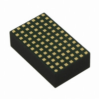
LTM4618IV#PBF Linear Technology, LTM4618IV#PBF Datasheet - Page 19

LTM4618IV#PBF
Manufacturer Part Number
LTM4618IV#PBF
Description
IC DC-DC UMODULE BUCK 6A 84-LGA
Manufacturer
Linear Technology
Series
µModuler
Type
Point of Load (POL) Non-Isolatedr
Datasheet
1.LTM4618EVPBF.pdf
(24 pages)
Specifications of LTM4618IV#PBF
Output
0.8 ~ 5 V
Number Of Outputs
1
Power (watts)
30W
Mounting Type
Surface Mount
Voltage - Input
4.5 ~ 26.5 V
Package / Case
84-LGA
1st Output
0.8 ~ 5 VDC @ 6A
Size / Dimension
0.59" L x 0.35" W x 0.17" H (15mm x 9mm x 4.32mm)
Power (watts) - Rated
30W
Operating Temperature
-40°C ~ 125°C
Lead Free Status / RoHS Status
Lead free / RoHS Compliant
3rd Output
-
2nd Output
-
Available stocks
Company
Part Number
Manufacturer
Quantity
Price
APPLICATIONS INFORMATION
EMI Section
The LTM4618 has been evaluated for CISPR22 A and B
Radiated EMI and CISPR25 Conducted EMI. The CISPR25
Conducted EMI test was performed with an input π fi lter
as shown in Figure 17. An RC snubber circuit is optionally
used from the SW pin to the PGND pin to improve the higher
frequency attenuation and EMI limit guard band. Figure 18
shows the CISPR25 conducted emissions plot for 26.5V
input to 3.3V output at 5A load. Several conditions were
evaluated, and Figure 18 results are from the worst-case
condition. The input π fi lter is used to attenuate the refl ected
noise from the regulator input, and is primarily utilized
when the power regulators are closed to the input power
feed to a board, like the input power connectors. If the
regulator design is placed out on the center of the system
board, then the input π fi lter may not be needed because
all of the extra board capacitance and the inductive planes
will provide fi ltering for refl ected emissions. If the system
board has noise sensitive circuitry that is powered from
the same voltage rail as the regulators are, then an input
π fi lter is a good idea to keep regulator noise from cor-
rupting the noise sensitive circuitry on the system board.
Figure 19 shows the CISPR22 B Radiated EMI plots. The
input π fi lter is used to attenuate the refl ected noise from
propagating out onto the input power cables, thus pos-
sibly causing radiated EMI issues. An RC snubber circuit
is optionally used from the SW pin to the PGND pin to
improve the higher frequency attenuation and EMI limit
guard band. A placeholder can accommodate the R
and C
components are probably not necessary, but can be used
or adjusted to improve the radiated limit guard bands at
the higher frequencies by attenuating any switch node
ringing due to parasitic values in the high speed switching
paths. It is important to follow the recommended layout
guidelines and use good X5R or X7R ceramic capacitors
to get good results.
Layout Checklist/Example
The high integration of LTM4618 makes the PC board layout
very simple and easy. However, to optimize its electrical
and thermal performance, some layout considerations
are still necessary.
SNUB
components with 1.2Ω and 470pF . These
SNUB
• Use large PCB copper areas for high current path,
• Test points can be placed on signal pin for monitor-
• Place high frequency ceramic input and output
• Place a dedicated power ground layer underneath the
• To minimize the via conduction loss and reduce mod-
• Do not put vias directly on the pad, unless they are
• Use a separated SGND ground copper area for com-
Figure 20 gives a good example of the recommended
layout.
CNTRL
including V
the PCB conduction loss and thermal stress.
ing during testing.
capacitors next to the V
minimize high frequency noise.
unit.
ule thermal stress, use multiple vias for interconnec-
tion between top layer and other power layers.
capped.
ponents connected to signal pins. Connect the SGND
to PGND underneath the unit.
V
7
6
5
4
3
2
1
IN
Figure 20. Recommended PCB Layout Example
A
B
IN
CNTRL
, PGND and V
C
D
PGND
E
IN
F
, PGND and V
OUT
G
. It helps to minimize
H
J
LTM4618
K
OUT
C
C
OUT
OUT
L
pins to
PGND
M
V
19
OUT
4618 F20
4618fa


