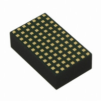
LTM4618IV#PBF Linear Technology, LTM4618IV#PBF Datasheet - Page 10

LTM4618IV#PBF
Manufacturer Part Number
LTM4618IV#PBF
Description
IC DC-DC UMODULE BUCK 6A 84-LGA
Manufacturer
Linear Technology
Series
µModuler
Type
Point of Load (POL) Non-Isolatedr
Datasheet
1.LTM4618EVPBF.pdf
(24 pages)
Specifications of LTM4618IV#PBF
Output
0.8 ~ 5 V
Number Of Outputs
1
Power (watts)
30W
Mounting Type
Surface Mount
Voltage - Input
4.5 ~ 26.5 V
Package / Case
84-LGA
1st Output
0.8 ~ 5 VDC @ 6A
Size / Dimension
0.59" L x 0.35" W x 0.17" H (15mm x 9mm x 4.32mm)
Power (watts) - Rated
30W
Operating Temperature
-40°C ~ 125°C
Lead Free Status / RoHS Status
Lead free / RoHS Compliant
3rd Output
-
2nd Output
-
Available stocks
Company
Part Number
Manufacturer
Quantity
Price
APPLICATIONS INFORMATION
LTM4618
The typical LTM4618 application circuit is shown in
Figure 21. External component selection is primarily
determined by the maximum load current and output
voltage.
V
There are restrictions in the maximum V
down ratio that can be achieved for a given input voltage.
One of the restrictions is the minimum on-time t
which is the smallest time duration that the LTM4618 can
operate. Make sure that the operating on-time is larger than
the minimum on-time as shown in the equation below. See
the Thermal Considerations and Output Current Derating
sections in this data sheet for the current restrictions.
t
Output Voltage Programming
The PWM controller has an internal 0.8V reference voltage.
As shown in the Block Diagram, a 60.4k internal feedback
resistor connects V
from the V
Table 1. V
V
R
10
ON(MIN)
OUT
FB
IN
t
V
(kΩ)
to V
ON(MIN)
(V)
OUT
OUT
is approximately 90ns, guardband to 110ns.
= 0.8V •
FB
Open
FB
0.8
Resistor Table vs Various Output Voltages
<
Step-Down Ratios
pin to SGND programs the output voltage:
V
V
IN
OUT
243
• ƒ
60.4k + R
1
OUT
R
to the V
121
FB
1.2
FB
69.8
1.5
FB
pin. Adding a resistor R
48.7
1.8
IN
28.7
2.5
to V
19.1
3.3
OUT
ON(MIN)
step-
11.5
5
FB
,
Input Capacitors
The LTM4618 module should be connected to a low AC-
impedance DC source. One 1.5μF input ceramic capacitor
is included inside the module. Additional input capacitors
are only needed if a large load step is required up to
the 6A level. A 47μF to 100μF surface mount aluminum
electrolytic bulk capacitor can be used for more input bulk
capacitance. This bulk input capacitor is only needed if
the input source impedance is compromised by long in-
ductive leads, traces or not enough source capacitance.
If low impedance power planes are used, then this 47μF
capacitor is not needed.
For a buck converter, the switching duty-cycle can be
estimated as:
Without considering the inductor current ripple, the RMS
current of the input capacitor can be estimated as:
In the above equation, η is the estimated effi ciency of
the power module. One 10μF ceramic input capacitor is
typically rated for 2A of RMS ripple current, so the RMS
input current at the worst case 6A maximum current is
about 3A. If a low inductance plane is used to power the
device, then two 10μF ceramic capacitors are enough for
the output at 6A load and no external input bulk capacitor
is required. The input RMS ripple current can be cancelled
by paralleling multiple LTM4618 power modules out of
phase, allowing the use of fewer input capacitors. Ap-
plication Note 77 explains the details.
I
D =
CIN(RMS)
V
V
OUT
IN
=
I
OUT(MAX)
η
• D • (1– D)
4618fa


