LTM4618IV#PBF Linear Technology, LTM4618IV#PBF Datasheet
LTM4618IV#PBF
Specifications of LTM4618IV#PBF
Available stocks


Related parts for LTM4618IV#PBF


LTM4618IV#PBF Summary of contents
Page 1
... The LTM4618 is Pb-free and RoHS compliant. L, LT, LTC, LTM, Linear Technology, the Linear logo, Burst Mode and μModule are registered trademarks and LTpowerCAD is a trademark of Linear Technology Corporation. All other trademarks are the property of their respective owners. ...
Page 2
... LEAD FREE FINISH PART MARKING* LTM4618EV#PBF LTM4618V LTM4618IV#PBF LTM4618V Consult LTC Marketing for parts specifi ed with wider operating temperature ranges. *The temperature grade is identifi label on the shipping container. For more information on lead free part marking, go to: This product is only offered in trays. For more information go to: ELECTRICAL CHARACTERISTICS operating temperature range, otherwise specifi ...
Page 3
ELECTRICAL CHARACTERISTICS operating temperature range, otherwise specifi cations are at T SYMBOL PARAMETER I Input Supply Bias Current Q(VIN) I Input Supply Current S(VIN) INTV Internal V Voltage EXTV Switchover Voltage EXTVCC CC VLDO External EXTV Voltage ...
Page 4
LTM4618 ELECTRICAL CHARACTERISTICS operating temperature range, otherwise specifi cations are at T SYMBOL PARAMETER f Highest Frequency HIGH V Synchronous Clock High Level IH(MODE/PLLIN) V Synchronous Clock Low Level IL(MODE/PLLIN) R MODE/PLLIN Input Resistance MODE/PLLIN I FREQ Pin FREQ Sinking ...
Page 5
TYPICAL PERFORMANCE CHARACTERISTICS Effi ciency vs Load Current with 5V (CCM) IN 100 0.8V OUT 5V TO 1.2V OUT 5V TO 1.5V 75 OUT 5V TO 2.5V OUT 5V TO 3.3V OUT 70 0 ...
Page 6
LTM4618 TYPICAL PERFORMANCE CHARACTERISTICS Start-Up OUT V OUT 1V/DIV I IN 0.2A/DIV 20ms/DIV V = 12V AND V = 2.5V IN OUT 22μF 6.3V CERAMIC, OUT 1 100μF 6.3V CERAMIC AND 1 220μF SANYO ...
Page 7
PIN FUNCTIONS NC (A1): No Connect. Leave fl oating. FREQ (A2): Frequency Selection Pin. An internal low pass fi lter is tied to this pin. The frequency can be selected with a voltage from this pin to SGND. A programming ...
Page 8
LTM4618 PIN FUNCTIONS additional decoupling of the 5V internal regulator. V (BANK 3: J1-J4, K1-K4, L1-L4, M1-M4): Power Out- OUT put Pins. Apply output load between these pins and PGND pins. Recommend placing output decoupling capacitance directly between these pins ...
Page 9
OPERATION Power Module Description The LTM4618 is a standalone non-isolated switching mode DC/DC power supply. It can deliver (DC current) output with few external input and output capacitors. This module provides precisely regulated output voltages pro- grammable ...
Page 10
LTM4618 APPLICATIONS INFORMATION The typical LTM4618 application circuit is shown in Figure 21. External component selection is primarily determined by the maximum load current and output voltage Step-Down Ratios IN OUT There are restrictions in the maximum ...
Page 11
... The table optimizes the total equivalent ESR and total bulk capacitance to optimize the transient performance. Stability criteria are considered in the Table 4 matrix, and the Linear Technology μModule Power Design Tool is available for stability analysis. Mul- tiphase operation will reduce effective output ripple as a function of the number of phases ...
Page 12
LTM4618 APPLICATIONS INFORMATION The LTM4618 can be synchronized from 400kHz to 780kHz with an input clock that has a high level above 2.0V and a low level below 0.8V. The 400kHz low end operation limit is put in place to ...
Page 13
APPLICATIONS INFORMATION Slope Compensation The module has already been internally compensated for all output voltages. LTpowerCAD is available for further control loop optimization. RUN Pin The RUN pin has a 1μA pull-up current source that will enable the device in ...
Page 14
LTM4618 APPLICATIONS INFORMATION board, and is really the sum of the θ thermal resistance of the bottom of the part through the solder joints and through a portion of the board. The board temperature is measured at specifi ed dis- ...
Page 15
APPLICATIONS INFORMATION The 1.5V and 3.3V power loss curves in Figures 7 and 8 can be used in coordination with the load current derating curves in Figures for calculating an approximate θ thermal resistance for the LTM4618 ...
Page 16
LTM4618 APPLICATIONS INFORMATION 0LFM 200LFM 400LFM 100 105 110 AMBIENT TEMPERATURE (°C) 4618 F09 Figure 1.5V without IN OUT Heat Sink ...
Page 17
APPLICATIONS INFORMATION Table 2. 1.5V Output DERATING CURVE V (V) IN Figures Figures Figures Figures 10 Figures 10 Figures 10 ...
Page 18
LTM4618 APPLICATIONS INFORMATION VISHAY INLP1616BZERR22M01 0.22μH π FILTER 26.5V 10μ • 1.22V Figure 17 26.5V Input, 3. Design, Meeting CISPR25 Conducted and ...
Page 19
APPLICATIONS INFORMATION EMI Section The LTM4618 has been evaluated for CISPR22 A and B Radiated EMI and CISPR25 Conducted EMI. The CISPR25 Conducted EMI test was performed with an input π fi lter as shown in Figure 17 ...
Page 20
LTM4618 TYPICAL APPLICATIONS 26. • 1.22V UVLO FUNCTION Figure 21. Typical 6V to 26.5V Input, 2. Design, 500kHz Operation 26. OUT1 C5 ...
Page 21
TYPICAL APPLICATIONS LTM4618 4618fa 21 ...
Page 22
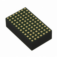
LTM4618 PACKAGE PHOTOGRAPH PACKAGE DESCRIPTION PIN NAME A1 N/C A2 FREQ A3 MODE/PLLIN A4 PGND TK/SS B2 RUN B3 SGND B4 PGND ...
Page 23
... PACKAGE DESCRIPTION Information furnished by Linear Technology Corporation is believed to be accurate and reliable. However, no responsibility is assumed for its use. Linear Technology Corporation makes no representa- tion that the interconnection of its circuits as described herein will not infringe on existing patent rights bbb 3.810 2.540 1.270 ...
Page 24
... Input, Dual 0. Output, PLL, Tracking 3.6V ≤ V ≤ 36V; 0.8V ≤ OUT www.linear.com ● 31.6k 10k CC V OUT OUT 2.5V/ OUT 47pF 100μ 28.7k ≤ 24V; 9mm × 15mm × 4.32mm LGA Package LT 0111 REV A • PRINTED IN USA © LINEAR TECHNOLOGY CORPORATION 2010 4618fa ...