AFCT-5961ATGZ Avago Technologies US Inc., AFCT-5961ATGZ Datasheet - Page 8
AFCT-5961ATGZ
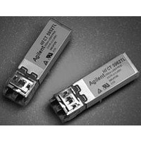
Manufacturer Part Number
AFCT-5961ATGZ
Description
TXRX OPT SM SONET OC3/SDH 2X5
Manufacturer
Avago Technologies US Inc.
Series
METRAKr
Datasheet
1.AFCT-5961TGZ.pdf
(16 pages)
Specifications of AFCT-5961ATGZ
Applications
General Purpose
Data Rate
155Mbps
Wavelength
1300nm
Voltage - Supply
3.1 V ~ 3.5 V
Connector Type
LC Duplex
Mounting Type
Through Hole
Data Rate Max
0.155Gbps
Supply Voltage
3.3V
Wavelength Typ
1300nm
Leaded Process Compatible
Yes
Optical Fiber Type
TX/RX
Data Transfer Rate
155Mbps
Optical Rise Time
2/2.2ns
Optical Fall Time
2/2.2ns
Operating Temperature Classification
Industrial
Peak Wavelength
1360nm
Package Type
DIP With Connector
Operating Supply Voltage (min)
3.1V
Operating Supply Voltage (typ)
3.3V
Operating Supply Voltage (max)
3.5V
Output Current
50mA
Operating Temp Range
-40C to 85C
Mounting
Snap Fit To Panel
Pin Count
10
Lead Free Status / RoHS Status
Lead free / RoHS Compliant
Lead Free Status / RoHS Status
Lead free / RoHS Compliant, Lead free / RoHS Compliant


Figure 6b. Recommended ac Coupled Interface Circuit
The AFCT-5961TLZ/TGZ/ATLZ/ATGZ/NLZ/NGZ have a
transmit disable function which is a single-ended +3.3 V
TTL input which is dc-coupled to pin 8.
As for the receiver section, it is internally ac-coupled
between the preamplifier and the postamplifier stages.
The actual Data and Data-bar outputs of the postampli-
fier are dc-coupled to their respective output pins (pins
4, 5). The two data outputs of the receiver should be ter-
minated with identical load circuits.
Signal Detect is a single-ended, +3.3 V PECL compatible
output signal that is dc-coupled to pin 3 of the module.
Signal Detect should not be ac-coupled externally to
the follow-on circuits because of its infrequent state
changes.
Power Supply Filtering and Ground Planes
It is important to exercise care in circuit board layout to
achieve optimum performance from these transceiv-
ers. Figures 6a and 6b show the power supply circuit
which complies with the small form factor multisource
agreement. It is further recommended that a continuous
8
T
Note: C1 = C2 = C3 = 10 nF or 100 nF
Note A: CIRCUIT ASSUMES OPEN EMITTER OUTPUT
Note B: WHEN INTERNAL BIAS IS PROVIDED REPLACE SPLIT RESISTORS WITH 100 W TERMINATION
* C4 AND C5 ARE OPTIONAL BYPASS CAPACITORS FOR ADDITIONAL LOW FREQUENCY NOISE FILTERING.
DIS
T
R
X
X
(LVTTL)
10
1
9
2
8
3
7
82 W
130 W
4
130 W
V
6
CC
5
(+3.3 V)
82 W
130 W
130 W
C2
C1
100 nF
1 µH
1 µH
100 nF
100 nF
100 nF
100 nF
C5 *
10 µF
C4 *
10 µF
ground plane be provided in the circuit board directly
under the transceiver to provide a low inductance ground
for signal return current. This recommendation is in
keeping with good high frequency board layout practices.
Package footprint and front panel considerations
The Avago Technologies transceivers comply with the
circuit board “Common Transceiver Footprint” hole
pattern defined in the current multisource agreement
which defined the 2 x 5 package style. This drawing
is reproduced in Figure 7 with the addition of ANSI
Y14.5M compliant dimensioning to be used as a guide
in the mechanical layout of your circuit board. Figure 8
shows the front panel dimensions associated with such
a layout.
Eye Safety Circuit
For an optical transmitter device to be eye-safe in the
event of a single fault failure, the transmitter must either
maintain eye-safe operation or be disabled.
The AFCT-5961TLZ/TGZ/ATLZ/ATGZ/NLZ/NGZ is intrinsi-
cally eye safe and does not require shut down circuitry.
Z = 50 W
Z = 50 W
Z = 50 W
Z = 50 W
Z = 50 W
V
CC
C3
(+3.3 V)
100 nF
100 nF
10 µF
130 W
82 W
130 W
V
130 W
82 W
CC
(+3.3 V)
V
CC
82 W
130 W
(+3.3 V)
RD+
TD-
TD+
RD-
SD
130
W
LVPECL
V
CC
V
(+3.3 V)
CC
(+3.3 V)
NOTE A
NOTE B
Related parts for AFCT-5961ATGZ
Image
Part Number
Description
Manufacturer
Datasheet
Request
R

Part Number:
Description:
TXRX OPT 1X9 155MB/S 1300NM BK
Manufacturer:
Avago Technologies US Inc.
Datasheet:

Part Number:
Description:
TXRX OPT SFF PLUGGABLE BAIL
Manufacturer:
Avago Technologies US Inc.
Datasheet:
Part Number:
Description:
TXRX OPT SFF PLUGGABLE BAIL DMI
Manufacturer:
Avago Technologies US Inc.
Datasheet:

Part Number:
Description:
TXRX 125MBD DUPLEX BLACK SC 1X9
Manufacturer:
Avago Technologies US Inc.
Datasheet:
Part Number:
Description:
TXRX 125MBD DUPLEX BLUE SC 1X9
Manufacturer:
Avago Technologies US Inc.
Datasheet:

Part Number:
Description:
TXRX OPT SM 155MBS SONET OC3/SDH
Manufacturer:
Avago Technologies US Inc.
Datasheet:
Part Number:
Description:
TXRX SFF SM OC3/STM-1 BAIL DMI
Manufacturer:
Avago Technologies US Inc.
Datasheet:
Part Number:
Description:
TXRX 125MBD DUPLEX BLACK SC 1X9
Manufacturer:
Avago Technologies US Inc.
Datasheet:
Part Number:
Description:
TXRX 125MBD DUPLEX BLUE SC 1X9
Manufacturer:
Avago Technologies US Inc.
Datasheet:

Part Number:
Description:
TXRX OPT SM 155MBS SONET OC3/SDH
Manufacturer:
Avago Technologies US Inc.
Datasheet:

Part Number:
Description:
OPTOCOUPLER GATE DRV 2A 16-SOIC
Manufacturer:
Avago Technologies US Inc.
Datasheet:
Part Number:
Description:
OPTOCOUPLER 2CH 2.5A 16-SOIC
Manufacturer:
Avago Technologies US Inc.
Datasheet:

Part Number:
Description:
OPTOCOUPLER GATE DRV 0.4A 16SOIC
Manufacturer:
Avago Technologies US Inc.
Datasheet:

Part Number:
Description:
OPTOCOUPLER 2.0A 250KHZ 8-DIP
Manufacturer:
Avago Technologies US Inc.
Datasheet:

Part Number:
Description:
OPTOCOUPLER 2.0A 250KHZ GW 8-SMD
Manufacturer:
Avago Technologies US Inc.
Datasheet: