AFBR-5905Z Avago Technologies US Inc., AFBR-5905Z Datasheet - Page 4
AFBR-5905Z
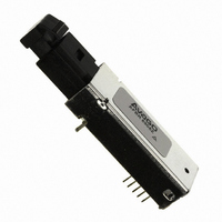
Manufacturer Part Number
AFBR-5905Z
Description
TXRX OPT OC3 MTRJ SFF 2X5DIP
Manufacturer
Avago Technologies US Inc.
Datasheet
1.AFBR-5905Z.pdf
(13 pages)
Specifications of AFBR-5905Z
Applications
General Purpose
Wavelength
1300nm
Voltage - Supply
3.3V
Connector Type
MTRJ
Mounting Type
Through Hole
Data Rate Max
0.1Gbps
Supply Voltage
3.3V
Wavelength Typ
1308nm
Leaded Process Compatible
Yes
Lead Free Status / RoHS Status
Lead free / RoHS Compliant
Data Rate
-
Lead Free Status / RoHS Status
Lead free / RoHS Compliant, Lead free / RoHS Compliant
Other names
516-1994


Pin Descriptions:
Pin 1 Receiver Signal Ground VEE RX:
Directly connect this pin to the receiver ground plane.
Pin 2 Receiver Power Supply VCC RX:
Provide +3.3 V dc via the recommended receiver power
supply filter circuit. Locate the power supply filter circuit
as close as possible to the VCC RX pin.
Pin 3 Signal Detect SD:
Normal optical input levels to the receiver result in a logic
“1” output. Low optical input levels to the receiver result in
a fault condition indicated by a logic “0” output. This Sig-
nal Detect output can be used to drive a PECL input on
an upstream circuit, such as Signal Detect input or Loss of
Signal-bar.
Pin 4 Receiver Data Out Bar RD-:
No internal terminations are provided. See recommended
circuit schematic.
Pin 5 Receiver Data Out RD+:
No internal terminations are provided. See recommended
circuit schematic.
44
Figure 3. Pin Out Diagram.
RECEIVER SIGNAL GROUND
Pin Descriptions:
Pin 1 Receiver Signal Ground V
Directly connect this pin to the
receiver ground plane.
Pin 2 Receiver Power Supply V
RX:
Provide +3.3 V dc via the
recommended receiver power
supply filter circuit. Locate
the power supply filter circuit
as close as possible to the V
RX pin.
Pin 3 Signal Detect SD:
Normal optical input levels to
the receiver result in a logic
“1” output.
Low optical input levels to the
receiver result in a fault
condition indicated by a logic
“0” output.
This Signal Detect output can
be used to drive a PECL input
on an upstream circuit, such
as Signal Detect input or Loss
of Signal-bar.
Pin 4 Receiver Data Out Bar RD-:
RECEIVER POWER SUPPLY
RECEIVER DATA OUT BAR
RECEIVER DATA OUT
SIGNAL DETECT
o
o
o
o
o
RX
1
2
3
4
5
EE
View
CC
Top
RX:
CC
TX
10
9
8
7
6
o
o
o
o
o
No internal terminations are
provided. See recommended
circuit schematic.
Pin 5 Receiver Data Out RD+:
No internal terminations are
provided. See recommended
circuit schematic.
Pin 6 Transmitter Power Supply
V
Provide +3.3 V dc via the
recommended transmitter
power supply filter circuit.
Locate the power supply filter
circuit as close as possible to
the V
Pin 7 Transmitter Signal Ground
V
Directly connect this pin to the
transmitter ground plane.
Pin 8 Transmitter Disable T
No internal connection.
Optional feature for laser
based products only. For laser
CC
EE
TX:
TRANSMITTER DATA IN BAR
TRANSMITTER DATA IN
TRANSMITTER DISABLE (LASER BASED PRODUCTS ONLY)
TRANSMITTER SIGNAL GROUND
TRANSMITTER POWER SUPPLY
TX:
CC
Mounting Studs/
Solder Posts
TX pin.
Pin 6 Transmitter Power Supply VCC TX:
Provide +3.3 V dc via the recommended transmitter power
supply filter circuit. Locate the power supply filter circuit
as close as possible to the VCC TX pin.
Pin 7 Transmitter Signal Ground VEE TX:
Directly connect this pin to the transmitter ground plane.
Pin 8 Transmitter Disable TDIS:
No internal connection. Optional feature for laser based
products only. For laser based products connect this pin
to +3.3 V TTL logic high “1” to disable module. To enable
module connect to TTL logic low “0”.
Pin 9 Transmitter Data In TD+:
No internal terminations are provided. See recommended
circuit schematic.
Pin 10 Transmitter Data In Bar TD-:
No internal terminations are provided. See recommended
circuit schematic.
Mounting Studs/Solder Posts
The mounting studs are provided for transceiver mechani-
cal attachment to the circuit board. It is recommended
that the holes in the circuit board be connected to chassis
ground.
DIS
:
based products connect this
pin to +3.3 V TTL logic high
“1” to disable module. To
enable module connect to TTL
logic low “0”.
Pin 9 Transmitter Data In TD+:
No internal terminations are
provided. See recommended
circuit schematic.
Pin 10 Transmitter Data In Bar TD-:
No internal terminations are
provided. See recommended
circuit schematic.
Mounting Studs/Solder Posts
The mounting studs are
provided for transceiver
mechanical attachment to the
circuit board. It is
recommended that the holes in
the circuit board be connected
to chassis ground.
Related parts for AFBR-5905Z
Image
Part Number
Description
Manufacturer
Datasheet
Request
R

Part Number:
Description:
650nm FE Transceiver Eval Kit
Manufacturer:
Avago Technologies US Inc.
Datasheet:

Part Number:
Description:
TXRX ETHERNET 125MBD MMF 2X5
Manufacturer:
Avago Technologies US Inc.
Datasheet:

Part Number:
Description:
TXRX OPT SFP DGTL 850NM IND
Manufacturer:
Avago Technologies US Inc.
Datasheet:

Part Number:
Description:
TXRX OPT SFF 4/2/1GBD 2X7
Manufacturer:
Avago Technologies US Inc.
Datasheet:

Part Number:
Description:
TXRX OPT SFP 4/2/1GBD 850NM
Manufacturer:
Avago Technologies US Inc.
Datasheet:

Part Number:
Description:
TXRX OPT XFP 10GB/S 850NM
Manufacturer:
Avago Technologies US Inc.
Datasheet:

Part Number:
Description:
TXRX OPT 1X9 100MBPS ST EXT TEMP
Manufacturer:
Avago Technologies US Inc.
Datasheet:

Part Number:
Description:
TXRX OPT 1X9 100MBPS SC EXT TEMP
Manufacturer:
Avago Technologies US Inc.
Datasheet:

Part Number:
Description:
TXRX OPT 1X9 100MBPS DUPLEX SC
Manufacturer:
Avago Technologies US Inc.
Datasheet:

Part Number:
Description:
TXRX OPT 1X9 100MBPS DUPLEX ST
Manufacturer:
Avago Technologies US Inc.
Datasheet:

Part Number:
Description:
OPTOCOUPLER GATE DRV 2A 16-SOIC
Manufacturer:
Avago Technologies US Inc.
Datasheet:
Part Number:
Description:
OPTOCOUPLER 2CH 2.5A 16-SOIC
Manufacturer:
Avago Technologies US Inc.
Datasheet:

Part Number:
Description:
OPTOCOUPLER GATE DRV 0.4A 16SOIC
Manufacturer:
Avago Technologies US Inc.
Datasheet:

Part Number:
Description:
OPTOCOUPLER 2.0A 250KHZ 8-DIP
Manufacturer:
Avago Technologies US Inc.
Datasheet:

Part Number:
Description:
OPTOCOUPLER 2.0A 250KHZ GW 8-SMD
Manufacturer:
Avago Technologies US Inc.
Datasheet: