AFBR-5905Z Avago Technologies US Inc., AFBR-5905Z Datasheet - Page 10
AFBR-5905Z
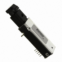
Manufacturer Part Number
AFBR-5905Z
Description
TXRX OPT OC3 MTRJ SFF 2X5DIP
Manufacturer
Avago Technologies US Inc.
Datasheet
1.AFBR-5905Z.pdf
(13 pages)
Specifications of AFBR-5905Z
Applications
General Purpose
Wavelength
1300nm
Voltage - Supply
3.3V
Connector Type
MTRJ
Mounting Type
Through Hole
Data Rate Max
0.1Gbps
Supply Voltage
3.3V
Wavelength Typ
1308nm
Leaded Process Compatible
Yes
Lead Free Status / RoHS Status
Lead free / RoHS Compliant
Data Rate
-
Lead Free Status / RoHS Status
Lead free / RoHS Compliant, Lead free / RoHS Compliant
Other names
516-1994


10
DIMENSIONS IN MILLIMETERS (INCHES)
Figure 10. Recommended Panel Mounting
Absolute Maximum Ratings
Stresses in excess of the absolute maximum ratings can cause catastrophic damage to the device. Limits apply to each parameter in
isolation, all other parameters having values within the recommended operating conditions. It should not be assumed that limiting values
of more than one parameter can be applied to the product at the same time. Exposure to the absolute maximum ratings for extended
periods can adversely affect device reliability.
Parameter
Lead Soldering Temperature
Lead Soldering Time
Data Input Voltage
Differential Input Voltage (p-p)
Storage Temperature
Supply Voltage
Output Current
10
(0.425 ±0.004)
10.8 ±0.1
(0.55)
13.97
MIN.
(TOP OF PCB TO
(0.01 ±0.004)
BOTTOM OF
OPENING)
0.25 ±0.1
(0.386 ±0.004)
9.8 ±0.1
(0.15)
3.8
Symbol
I
T
T
t
V
V
V
(0.039)
O
SOLD
S
SOLD
CC
I
D
(0.589)
14.79
1
Minimum Typical
-40
-0.5
-0.5
Figure 11. Transmitter Output Optical Spectral
Width (FWHM) vs. Transmitter Output Optical
Center Wavelength and Rise/Fall Times.
Figure 12. Relative Input Optical Power vs.
Eye Sampling Time Position.
Maximum Unit
+100
+260
10
3.6
2.0
50
V
CC
200
180
160
140
120
100
1260
6
5
4
3
2
1
0
-3
HFBR-5905 TRANSMITTER TEST RESULTS
OF λ
WITH THE ALLOWED SPECTRAL WIDTH AS A FUNCTION
OF CENTER WAVELENGTH FOR VARIOUS RISE AND
FALL TIMES.
CONDITIONS:
1. T
2. V
3. INPUT OPTICAL RISE/FALL TIMES = 1.0/2.1 ns.
4. INPUT OPTICAL POWER IS NORMALIZED TO
5. NOTE 15 AND 16 APPLY.
CENTER OF DATA SYMBOL.
λ
TIMES – ns
A
CC
C
C
1.0
1.5
2.0
2.5
3.0
= +25 C
, ∆λ AND t
– TRANSMITTER OUTPUT OPTICAL RISE/FALL
= 3.3 V dc
1280
-2
EYE SAMPLING TIME POSITION (ns)
mA
°C
°C
sec.
V
V
V
r/f
-1
1300
ARE CORRELATED AND COMPLY
t
OUTPUT OPTICAL RISE/
FALL TIMES – ns
r/f
0
– TRANSMITTER
Reference
Note 1
1320
1
1340
2
3.0
1360
3
Related parts for AFBR-5905Z
Image
Part Number
Description
Manufacturer
Datasheet
Request
R

Part Number:
Description:
650nm FE Transceiver Eval Kit
Manufacturer:
Avago Technologies US Inc.
Datasheet:

Part Number:
Description:
TXRX ETHERNET 125MBD MMF 2X5
Manufacturer:
Avago Technologies US Inc.
Datasheet:

Part Number:
Description:
TXRX OPT SFP DGTL 850NM IND
Manufacturer:
Avago Technologies US Inc.
Datasheet:

Part Number:
Description:
TXRX OPT SFF 4/2/1GBD 2X7
Manufacturer:
Avago Technologies US Inc.
Datasheet:

Part Number:
Description:
TXRX OPT SFP 4/2/1GBD 850NM
Manufacturer:
Avago Technologies US Inc.
Datasheet:

Part Number:
Description:
TXRX OPT XFP 10GB/S 850NM
Manufacturer:
Avago Technologies US Inc.
Datasheet:

Part Number:
Description:
TXRX OPT 1X9 100MBPS ST EXT TEMP
Manufacturer:
Avago Technologies US Inc.
Datasheet:

Part Number:
Description:
TXRX OPT 1X9 100MBPS SC EXT TEMP
Manufacturer:
Avago Technologies US Inc.
Datasheet:

Part Number:
Description:
TXRX OPT 1X9 100MBPS DUPLEX SC
Manufacturer:
Avago Technologies US Inc.
Datasheet:

Part Number:
Description:
TXRX OPT 1X9 100MBPS DUPLEX ST
Manufacturer:
Avago Technologies US Inc.
Datasheet:

Part Number:
Description:
OPTOCOUPLER GATE DRV 2A 16-SOIC
Manufacturer:
Avago Technologies US Inc.
Datasheet:
Part Number:
Description:
OPTOCOUPLER 2CH 2.5A 16-SOIC
Manufacturer:
Avago Technologies US Inc.
Datasheet:

Part Number:
Description:
OPTOCOUPLER GATE DRV 0.4A 16SOIC
Manufacturer:
Avago Technologies US Inc.
Datasheet:

Part Number:
Description:
OPTOCOUPLER 2.0A 250KHZ 8-DIP
Manufacturer:
Avago Technologies US Inc.
Datasheet:

Part Number:
Description:
OPTOCOUPLER 2.0A 250KHZ GW 8-SMD
Manufacturer:
Avago Technologies US Inc.
Datasheet: