M0240SD-402MDAR1-3 Newhaven Display, M0240SD-402MDAR1-3 Datasheet - Page 9
M0240SD-402MDAR1-3
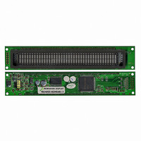
Manufacturer Part Number
M0240SD-402MDAR1-3
Description
MODULE VF CHAR 2X40 5.34MM
Manufacturer
Newhaven Display
Datasheet
1.M0240SD-402MDAR1-3.pdf
(21 pages)
Specifications of M0240SD-402MDAR1-3
Outline L X W X H
182.00mm x 33.50mm x 17.60mm
Viewing Area
134.75mm L x 11.50mm W
Display Format
40 x 2
Display Type
Character
Format
5 x 8 Dots
Voltage - Supply
4.5 V ~ 5.5 V
Character Size
5.34mm H x 2.10mm W
Interface
Parallel
Operating Temperature
-20°C ~ 70°C
Product
Character Display Modules
Character Count X Line
40 x 2
Module Size (w X H X T)
182 mm x 33.5 mm x 17.6 mm
Voltage Rating
4.5 V to 5.5 V
Operating Temperature Range
- 20 C to + 70 C
Dot Format
5 x 8
Viewing Area (w X H)
134.75 mm x 11.5 mm
Lead Free Status / RoHS Status
Lead free / RoHS Compliant
Number Of Dots
-
Lead Free Status / Rohs Status
Details


STANDARD
NAME
5.1.1 Busy Flag (BF)
5.1.2 Address Counter (ACC)
5.1.3 Display Data RAM (DD-RAM)
5.1.4 Character Generator ROM (CG-ROM)
5.1.5 Character Generator RAM (CG-RAM)
Table-8 Register Selection
1
2nd
RS
Table-9 Relation between Digit Position and DD-RAM data
0
0
1
1
st
The address counter (ACC) assigns addresses to both DD-RAM and CG-RAM. When an address of an
When the busy flag is 1, the controller is in the internal operation mode, and the next instruction will
instruction is written into the IR, the address information is sent from the IR to the ACC. Selection of
either DD-RAM or CG-RAM is also determined concurrently by the instruction. After writing into
(reading from) DD-RAM or CG-RAM, the ACC is automatically incremented by 1 (decremented by
1). The ACC contents are then output to Db0 to Db6 when RS =0 and R/W=1 (See Table-8).
not be accepted. When RS =0 and R/W=1 (Table-8), the busy flag is output to DB7.
The next instruction must be written after ensuring that the busy flag is 0.
Row
The character generator ROM (CG-ROM) generates character patterns of 5x8 dots from 8-bit character
The character fonts are shown on the following page. The character codes 00H to 0FH are allocated to
rewrite character patterns by program.
written. Write into DD-RAM the character codes at the
addresses shown as the left column of Table-10 to show
the character patterns stored in CG-RAM.
addresses and data and display patterns and refer to
Fig-10 for dot assignment of VFD.
Display data RAM (DD-RAM) stores display data represented in 8-bit character codes.
The area in DD-RAM that is not used for display can be used as general data RAM.
See Table-9 for the relationships between DD-RAM addresses and positions on the VFD
In the character generator RAM (CG-RAM), the user can
For 5 8 dots and cursor, eight character patterns can be
See Table-11 for the relationship between CG-RAM
Areas that are not used for display can be used as general data RAM
the CG-RAM.
codes (table-10). It can generate 240 kinds of 5x8 dots character patterns.
M68
R/W
0
1
0
1
Left End
00H
40H
/RD
1
0
1
0
i80
/WR
2
41H
01H
0
1
0
1
nd
Column
IR write as an internal operation (display clear, ect.)
Read busy flag (DB7) and address counter (DB0 to DB6)
DR write as an internal operation (DR to DD-RAM or CG-RAM)
DR read as an internal operation (DD-RAM or CG-RAM to DR)
3
42H
02H
rd
column
- - - - - - - - - - -
- - - - - - - - -- - -
- - - - - - - - -- - -
Operation
DOCUMENT NO.
39
1
6
11
16
21
26
31
36
26H
66H
th
Column Right End
37
2
7
12
17
22
27
32
38
3
8
13
18
23
28
33
REV.NO
00
27H
67H
4
9
14
19
24
29
34
39
5
10
15
20
25
30
35
40
PAGE
8/20
Related parts for M0240SD-402MDAR1-3
Image
Part Number
Description
Manufacturer
Datasheet
Request
R

Part Number:
Description:
DISPLAY VFD ALPHA 1X20 6.5MM
Manufacturer:
Newhaven Display
Datasheet:

Part Number:
Description:
DISPLAY VFD ALPHA 1X16 5MM
Manufacturer:
Newhaven Display
Datasheet:

Part Number:
Description:
DISPLAY VFD 7-SEG 1X9 9.7MM
Manufacturer:
Newhaven Display
Datasheet:

Part Number:
Description:
DISPLAY VFD 7-SEG 1X6 20MM
Manufacturer:
Newhaven Display
Datasheet:

Part Number:
Description:
DISPLAY VFD 7-SEG 1X19 11MM
Manufacturer:
Newhaven Display
Datasheet:

Part Number:
Description:
DISPLAY VFD 7-SEG 1X3 8MM
Manufacturer:
Newhaven Display
Datasheet:

Part Number:
Description:
DISPLAY VFD CUSTOM DVD
Manufacturer:
Newhaven Display
Datasheet:

Part Number:
Description:
DISPLAY VFD CUST AUDIO
Manufacturer:
Newhaven Display
Datasheet:

Part Number:
Description:
DISPLAY VFD CUST AUDIO
Manufacturer:
Newhaven Display
Datasheet:

Part Number:
Description:
DISPLAY VFD 7-SEG 1X5 7.6MM
Manufacturer:
Newhaven Display
Datasheet:

Part Number:
Description:
DISPLAY VFD CUST APPLIANCE
Manufacturer:
Newhaven Display
Datasheet:

Part Number:
Description:
DISPLAY VFD CUSTOM DVD
Manufacturer:
Newhaven Display
Datasheet:

Part Number:
Description:
DISPLAY VFD 7-SEG 1X4 7.6MM
Manufacturer:
Newhaven Display
Datasheet:

Part Number:
Description:
DISPLAY VFD 7-SEG 1X9 8MM
Manufacturer:
Newhaven Display
Datasheet:

Part Number:
Description:
DISPLAY VFD 7-SEG 1X7 12.5MM
Manufacturer:
Newhaven Display
Datasheet: