M0240SD-402MDAR1-3 Newhaven Display, M0240SD-402MDAR1-3 Datasheet
M0240SD-402MDAR1-3
Specifications of M0240SD-402MDAR1-3


Related parts for M0240SD-402MDAR1-3


M0240SD-402MDAR1-3 Summary of contents
Page 1
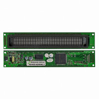
... M0240SD‐402MDAR1‐3 Vacuum Fluorescent Display Module RoHS Compliant ...
Page 2
STARDARD NAME Document Revision History Revision Date 0 7/27/2003 1 3/25/2011 DOCUMENT NO. Description Initial Release Mechanical drawing updated REV NO. PAGE 1/20 Changed By ‐ AK ...
Page 3
... STANDARD NAME 1. SCOPE This specification applies to VFD module (Model No: M0240SD-402MDA1-3) 2. FEATURES 2.1 LCD compatible interface and mounting holes. (This VFD module is capable to communicate some different type of bus systems such as i80 (Intel) or M68 (Motorola), 8-bit or 4-bit parallel data.) 2.2 High quality of display and luminance. ...
Page 4
STANDARD NAME Display size Number of digit Character Size Character Pitch Dot Size Display color 4.4 Environment Conditions Parameter Operating temperature Storage temperature Humidity(operating) Humidity(non-operating) Vibration(5-55hz) shock 4.5 Absolute Maximum Ratings Parameter Supply voltage Input signal voltage 4.6 Recommend Operating ...
Page 5
STANDARD NAME 4.8 Timing Chart and AC Characteristics 4.8.1 Power-on Reset and /or REST Signal Timing T M 0.2V 4.8.2 I80 type CPU bus write in Timing RS T str(RS) Min 10ns /WR DB0-DB7 4.8.3 i80 type CPU bus read-out ...
Page 6
STANDARD NAME 4.8.4 M68 type CPU bus write in timing Fig-4 Data write-in Timing Diagram(M68 bus interface) 4.8.5 M68 type CPU bus read-out Timing R/W T sh(rs,r/ cyc M ax 160ns DB0-DB7 Fig-5 Data read-out Timing ...
Page 7
STANDARD NAME 4.9 SYSTEM BLOCK DIAGRAM Fig-6 System Block Diagram of this VFD Module 4.10 Outer Dimensions DOCUMENT NO. Fig-7 Outer dimensions REV. NO. PAGE 00 6/20 ...
Page 8
STANDARD NAME 4.11 Connecter Through Hole Location 4.12 Pattern Details 5.FUNCTION DESCRIPTIONS 5.1 Registers in VFD Controlle The VFD controller has two 8-bit registers, an instruction register (IR) and a data register (DR). IR stores instruction codes, such as display ...
Page 9
STANDARD NAME Table-8 Register Selection M68 i80 RS R/W /RD / 5.1.1 Busy Flag (BF) When the busy flag is 1, the controller is ...
Page 10
STANDARD NAME Table-10 Characters Font Table (CG-ROM)and CG-RAM codes ...
Page 11
STANDARD NAME Table-11 Relationship between CG-RAM address, Character Codes (DD-RAM) AND 5*8 Dot Character Patterns (CG-RAM) Character Codes (DD-RAM DATA ...
Page 12
STANDARD NAME allowing interfacing with 4-bit or 8-bit MPUs. For 4-bit interface data, only four bus lines (DB4 to DB7) are used for transfer. When to use 4-bit parallel data transfer, DB0 to DB3 keep “H”or “L”. The data transfer ...
Page 13
STANDARD NAME 3) Display on/off control: D=0; Display off B=0; Blinking off C=0; Cursor off 4) Entry mode set: L/D=1; Increment by 1 S=0; No shift 5) Function set IF=1; 8-bit interface data BR0=BR1=0; Brightness=100% N=1; 2-line display 6) CPU ...
Page 14
STANDARD NAME 6.1 Outline Only the instruction register (IR) and data register (DR) of the VFD controller can be controlled by the user's MPU. Before starting the internal operation of the controller, control information is temporarily stored into these registers ...
Page 15
STANDARD NAME Table –13 Instruction Set Instruction RS R/W Display clear 0 0 Cursor Home 0 0 Entry Mode set 0 0 Display ON/OFF 0 0 Control Cursor or display 0 0 Shift Function set 0 0 CGRAM address 0 ...
Page 16
STANDARD NAME Data write DDRAM Data Read from DDRAM I/D=1: Increment I/D=0: Decrement S=1: Display shift enabled S=0: Cursor shift enabled S/C=1: Display shift S/C=0: Cursor move R/L=1: Shift to the ...
Page 17
STANDARD NAME 6.2.2 Cursor Home DB7 DB6 DB5 DB4 DB3 DB2 DB1 DB0 RS=0, R/W=0 This instruction (1) Clears the contents of the address counter (ACC) to 00H. (2) Sets the address counter (ACC) to point to ...
Page 18
STANDARD NAME 6.2.4 Display ON/OFF DB7 DB6 DB5 DB4 RS=0, R/W=0 This instruction controls various features of the display. D=1: Display on , C=1: Cursor on B=1: Blinking on (Blinking is achieved by alternating between a normal ...
Page 19
STANDARD `NAME 6.2.6.Function Set DB7 DB6 DB5 DB4 RS=0, R/W=0 This instruction sets width of data bus line.(when to use parallel interface. IM=1). The number of display line and brightness control. This instruction initializes the system, and ...
Page 20
STANDARD NAME This instruction (1) Loads a new 7-bit address into the address counter (ACC). (2) Sets the address counter (ACC) to point to the DD-RAM. Once the “Set DD-RAM Address” instruction has been executed, the contents of the address ...
Page 21
STANDARD NAME Note: The address counter (ACC) is automatically incremented or decremented by 1 after the write instructions to CG-RAM or DD-RAM are executed. The RAM data selected by the ACC cannot be read out at this time even if ...