M0240SD-402MDAR1-3 Newhaven Display, M0240SD-402MDAR1-3 Datasheet - Page 20
M0240SD-402MDAR1-3
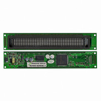
Manufacturer Part Number
M0240SD-402MDAR1-3
Description
MODULE VF CHAR 2X40 5.34MM
Manufacturer
Newhaven Display
Datasheet
1.M0240SD-402MDAR1-3.pdf
(21 pages)
Specifications of M0240SD-402MDAR1-3
Outline L X W X H
182.00mm x 33.50mm x 17.60mm
Viewing Area
134.75mm L x 11.50mm W
Display Format
40 x 2
Display Type
Character
Format
5 x 8 Dots
Voltage - Supply
4.5 V ~ 5.5 V
Character Size
5.34mm H x 2.10mm W
Interface
Parallel
Operating Temperature
-20°C ~ 70°C
Product
Character Display Modules
Character Count X Line
40 x 2
Module Size (w X H X T)
182 mm x 33.5 mm x 17.6 mm
Voltage Rating
4.5 V to 5.5 V
Operating Temperature Range
- 20 C to + 70 C
Dot Format
5 x 8
Viewing Area (w X H)
134.75 mm x 11.5 mm
Lead Free Status / RoHS Status
Lead free / RoHS Compliant
Number Of Dots
-
Lead Free Status / Rohs Status
Details


STANDARD
NAME
6.2.9 Read Busy Flag and Address
(1) Loads a new 7-bit address into the address counter (ACC).
(2) Sets the address counter (ACC) to point to the DD-RAM.
Once the “Set DD-RAM Address” instruction has been executed, the contents of the address counter (ACC)
will be automatically modified after each access of DD-RAM, as selected by the “Entry Mode Set”
instruction.
Table-16 Valid DD-RAM address Ranges
The next instruction will not be accepted until BF is reset to 0.Check the BF status before the next write
operation. At the same time, the value of the address counter (ACC) in binary AAAAAAA is read out. This
address counter (ACC) is used by both CG-RAM and DD-RAM address and its value is determined by the
previous instruction. The address counter are the same as for instructions set CG-RAM address and set
DD-RAM address.
This instruction writes 8-bit binary data (DB7 to DB0) from CG-RAM or DD-RAM.
The previous designation determines whether CG-RAM or DD-RAM is to be read.
Before entering this read instruction, either CG-RAM or DD-RAM address set instruction must be
executed. If not executed, the first read data will be invalid. When serially executing read instructions, the
next address data is normally read from the second read. The address set instructions need not be executed
just before this read instruction when shifting the cursor shift instruction (when reading out DD-RAM).
The operation of the cursor shift instruction is the same as the set DD-RAM address instruction.
After a read, the entry mode automatically increases or decreases the address by 1.
This instruction
RS=0, R/W=1
RS=1, R/W=0
DB7 DB6 DB5 DB4
DB7 DB6 DB5
BF
2
1
nd
st
line
line
Data Read
Number of Character
DB4
DB3 DB2 DB1 DB0
ACC
DB3 DB2 DB1 DB0
40
40
Address Range
00H to 27H
40H to 67H
DOCUMENT NO.
REV.NO
00
19/20
PAGE
Related parts for M0240SD-402MDAR1-3
Image
Part Number
Description
Manufacturer
Datasheet
Request
R

Part Number:
Description:
DISPLAY VFD ALPHA 1X20 6.5MM
Manufacturer:
Newhaven Display
Datasheet:

Part Number:
Description:
DISPLAY VFD ALPHA 1X16 5MM
Manufacturer:
Newhaven Display
Datasheet:

Part Number:
Description:
DISPLAY VFD 7-SEG 1X9 9.7MM
Manufacturer:
Newhaven Display
Datasheet:

Part Number:
Description:
DISPLAY VFD 7-SEG 1X6 20MM
Manufacturer:
Newhaven Display
Datasheet:

Part Number:
Description:
DISPLAY VFD 7-SEG 1X19 11MM
Manufacturer:
Newhaven Display
Datasheet:

Part Number:
Description:
DISPLAY VFD 7-SEG 1X3 8MM
Manufacturer:
Newhaven Display
Datasheet:

Part Number:
Description:
DISPLAY VFD CUSTOM DVD
Manufacturer:
Newhaven Display
Datasheet:

Part Number:
Description:
DISPLAY VFD CUST AUDIO
Manufacturer:
Newhaven Display
Datasheet:

Part Number:
Description:
DISPLAY VFD CUST AUDIO
Manufacturer:
Newhaven Display
Datasheet:

Part Number:
Description:
DISPLAY VFD 7-SEG 1X5 7.6MM
Manufacturer:
Newhaven Display
Datasheet:

Part Number:
Description:
DISPLAY VFD CUST APPLIANCE
Manufacturer:
Newhaven Display
Datasheet:

Part Number:
Description:
DISPLAY VFD CUSTOM DVD
Manufacturer:
Newhaven Display
Datasheet:

Part Number:
Description:
DISPLAY VFD 7-SEG 1X4 7.6MM
Manufacturer:
Newhaven Display
Datasheet:

Part Number:
Description:
DISPLAY VFD 7-SEG 1X9 8MM
Manufacturer:
Newhaven Display
Datasheet:

Part Number:
Description:
DISPLAY VFD 7-SEG 1X7 12.5MM
Manufacturer:
Newhaven Display
Datasheet: