MT9HTF6472AY-667D4 Micron Technology Inc, MT9HTF6472AY-667D4 Datasheet - Page 35

MT9HTF6472AY-667D4
Manufacturer Part Number
MT9HTF6472AY-667D4
Description
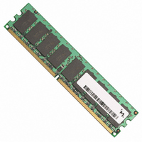
MODULE DDR2 512MB 240-DIMM
Manufacturer
Micron Technology Inc
Datasheet
1.MT9HTF12872AY-40ED1.pdf
(44 pages)
Specifications of MT9HTF6472AY-667D4
Memory Type
DDR2 SDRAM
Memory Size
512MB
Package / Case
240-DIMM
Lead Free Status / RoHS Status
Lead free / RoHS Compliant
Speed
-
Other names
557-1303
MT9HTF6472AY-667D4
MT9HTF6472AY-667D4
Notes
pdf: 09005aef80e6f860, source: 09005aef80e5b799
HTF9C32_64_128x72AG_2.fm - Rev. C 6/05 EN
10.
11. The intent of the Don’t Care state after completion of the postamble is the DQS-driven
12. This is not a device limit. The device will operate with a negative value, but system
1. All voltages referenced to V
2. Tests for AC timing,
3. Outputs measured with equivalent load:
4. AC timing and
5. The AC and DC input level specifications are as defined in the SSTL_18 standard (i.e.,
6. Command/Address minimum input slew rate is at 1.0V/ns. Command/Address input
7. Data minimum input slew rate is at 1.0V/ns. Data input timing must be derated if the
8.
9. This maximum value is derived from the referenced test load.
Output
(V
OUT
nominal reference/supply voltage levels, but the related specifications and device
operation are guaranteed for the full voltage range specified.
ment and parameter specifications are guaranteed for the specified AC input levels
under normal use conditions. The minimum slew rate for the input signals used to
test the device is 1.0V/ns for signals in the range between V
rates less than 1.0V/ns require the timing parameters to be derated as specified.
the receiver will effectively switch as a result of the signal crossing the AC input level
and will remain in that state as long as the signal does not ring back above [below] the
DC input LOW [HIGH] level).
timing must be derated if the slew rate is not 1.0V/ns. This is easily accommodated
using
enced from V
is referenced from V
table also lists the
ues.
slew rate is not 1.0V/ns. This is easily accommodated if the timing is referenced from
the logic trip points.
and V
ing signal and V
ues for a 1.0V/ns slew rate. If the DQS/DQS# differential strobe feature is not enabled,
timing is no longer referenced to the crosspoint of DQS/DQS#. Data timing is now ref-
erenced to V
rate is less than 1.0V/ns, then data timing is now referenced to V
DQS and V
t
tions. These parameters are not referenced to a specific voltage level, but specify
when the device output is no longer driving (
over
t
signal should either be high, low or High-Z and that any signal transition within the
input switching region must follow valid input requirements. That is if DQS transi-
tions high (above V
t
performance could be degraded due to bus turnaround.
HZ and
LZ (MIN) will prevail over a
DQSH (MIN).
256MB, 512MB, 1GB (x72, SR, ECC) 240-Pin DDR2 SDRAM UDIMM
)
V
TT =
t
DQSCK (MAX) +
IL
t
V
IS
DD
25Ω
(AC) for a falling signal.
b
t
Q/2
LZ transitions occur in the same access time windows as valid data transi-
and the Setup and Hold Time Derating Values table.
IL
Reference
Point
REF
(
DC
IH
I
, provided the DQS slew rate is not less than 1.0V/ns. If the DQS slew
DD
(
IL
) for a falling DQS.
AC
(
t
DC
tests may use a V
IS
) for a rising signal and V
IH
I
IH
DD
b
) for a falling signal. The timing table lists the
t
DC(min) then it must not transition low (below V
DS timing (
(
t
and
, and electrical AC and DC characteristics may be conducted at
AC
RPST (MAX) condition.
) for a rising signal and V
t
35
SS
IH
t
.
DQSCK (MIN) +
b
values for a 1.0V/ns slew rate; these are the “base” val-
t
IH timing (
t
DS
IL
Micron Technology, Inc., reserves the right to change products or specifications without notice.
b
-to-V
) is referenced from V
IH
t
IL
IH
t
HZ) or begins driving (
(
t
swing of up to 1.0V in the test environ-
RPRE (MAX) condition.
AC
b
) is referenced from V
) for a falling signal.
IL
(
DC
©2003, 2004, 2005 Micron Technology, Inc. All rights reserved.
) for a falling signal. The timing
IL
IH
(AC) and V
t
IS timing (
(AC) for a rising signal
t
HZ (MAX) will prevail
t
DS
IH
t
LZ).
t
IH timing (
(
IH
b
AC
IH
(DC) for a ris-
and
(DC) prior to
IH
) for a rising
t
IS
(AC). Slew
b
t
) is refer-
DH
Notes
b
t
IH
val-
b
)


