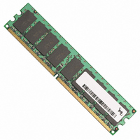
MT9HTF6472AY-667D4 Micron Technology Inc, MT9HTF6472AY-667D4 Datasheet - Page 15

MT9HTF6472AY-667D4
Manufacturer Part Number
MT9HTF6472AY-667D4
Description
MODULE DDR2 512MB 240-DIMM
Manufacturer
Micron Technology Inc
Datasheet
1.MT9HTF12872AY-40ED1.pdf
(44 pages)
Specifications of MT9HTF6472AY-667D4
Memory Type
DDR2 SDRAM
Memory Size
512MB
Package / Case
240-DIMM
Lead Free Status / RoHS Status
Lead free / RoHS Compliant
Speed
-
Other names
557-1303
MT9HTF6472AY-667D4
MT9HTF6472AY-667D4
Table 6:
Operating Mode
DLL Reset
Write Recovery
pdf: 09005aef80e6f860, source: 09005aef80e5b799
HTF9C32_64_128x72AG_2.fm - Rev. C 6/05 EN
Burst Definition
The normal operating mode is selected by issuing a LOAD MODE command with bit M7
set to zero, and all other bits set to the desired values as shown in Figure 5, Mode Register
(MR) Definition, on page 14. When bit M7 is ‘1,’ no other bits of the mode register are
programmed. Programming bit M7 to ‘1’ places the DDR2 SDRAM device into a test
mode that is only used by the Manufacturer and should NOT be used. No operation or
functionality is guaranteed if M7 bit is ‘1.’
DLL reset is defined by bit M8 as shown in Figure 5, Mode Register (MR) Definition, on
page 14. Programming bit M8 to ‘1’ will activate the DLL RESET function. Bit M8 is self-
clearing, meaning it returns back to a value of ‘0’ after the DLL RESET function has been
issued.
Anytime the DLL RESET function is used, 200 clock cycles must occur before a READ
command can be issued to allow time for the internal clock to be synchronized with the
external clock. Failing to wait for synchronization to occur may result in a violation of
the
Write recovery (WR) time is defined by bits M9–M11 as shown in Figure 5, Mode Register
(MR) Definition, on page 14. The WR Register is used by the DDR2 SDRAM device during
WRITE with AUTO PRECHARGE operation. During WRITE with AUTO PRECHARGE
operation, the DDR2 SDRAM device delays the internal AUTO PRECHARGE operation
by WR clocks (programmed in bits M9–M11) from the last data burst.
Write Recovery (WR) values of 2, 3, 4, 5, or 6 clocks may be used for programming bits
M9–M11. The user is required to program the value of write recovery, which is calculated
by dividing
integer; WR [cycles] =
unknown operation or incompatibility with future versions may result.
Burst Length
t
256MB, 512MB, 1GB (x72, SR, ECC) 240-Pin DDR2 SDRAM UDIMM
AC or
4
8
t
DQSCK parameters.
t
WR (in ns) by
Starting Column
(A2, A1, A0)
Address
t
WR [ns] /
0 0 0
0 0 1
0 1 0
0 1 1
0 0 0
0 0 1
0 1 0
0 1 1
1 0 0
1 0 1
1 1 0
1 1 1
t
CK (in ns) and rounding up a noninteger value to the next
15
t
CK [ns]. Reserved states should not be used as
Burst Type = Sequential Burst Type = Interleaved
Micron Technology, Inc., reserves the right to change products or specifications without notice.
0,1,2,3,4,5,6,7
1,2,3,0,5,6,7,4
2,3,0,1,6,7,4,5
3,0,1,2,7,4,5,6
4,5,6,7,0,1,2,3
5,6,7,4,1,2,3,0
6,7,4,5,2,3,0,1
7,4,5,6,3,0,1,2
Order of Accesses Within a Burst
0,1,2,3
1,2,3,0
2,3,0,1
3,0,1,2
©2003, 2004, 2005 Micron Technology, Inc. All rights reserved.
Mode Register (MR)
0,1,2,3,4,5,6,7
1,0,3,2,5,4,7,6
2,3,0,1,6,7,4,5
3,2,1,0,7,6,5,4
4,5,6,7,0,1,2,3
5,4,7,6,1,0,3,2
6,7,4,5,2,3,0,1
7,6,5,4,3,2,1,0
0,1,2,3
1,0,3,2
2,3,0,1
3,2,1,0


