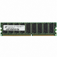
MT9VDDT6472AY-40BF1 Micron Technology Inc, MT9VDDT6472AY-40BF1 Datasheet - Page 19

MT9VDDT6472AY-40BF1
Manufacturer Part Number
MT9VDDT6472AY-40BF1
Description
MODULE DDR SDRAM 512MB 184-DIMM
Manufacturer
Micron Technology Inc
Datasheet
1.MT9VDDT6472AY-40BF1.pdf
(27 pages)
Specifications of MT9VDDT6472AY-40BF1
Memory Type
DDR SDRAM
Memory Size
512MB
Speed
400MT/s
Package / Case
184-DIMM
Lead Free Status / RoHS Status
Lead free / RoHS Compliant
Other names
557-1178
MT9VDDT6472AY-40BF1
MT9VDDT6472AY-40BF1
pdf: 09005aef80a43e7d, source: 09005aef80a43d77
DDA9C16_32_64x72AG.fm - Rev. B 9/04 EN
23. Each byte lane has a corresponding DQS.
24. This limit is actually a nominal value and does not
25. To maintain a valid level, the transitioning edge of
26. CK and CK# input slew rate must be
27. DQ and DM input slew rates must not deviate from
28. V
29. The clock is allowed up to ±150ps of jitter. Each
30.
31. READs and WRITEs with auto precharge are not
160
140
120
100
80
60
40
20
Figure 7: Pull-Down Characteristics
0
0.0
(
in direct proportion to the clock duty cycle and a
practical data valid window can be derived. The
clock is allowed a maximum duty cycle variation of
45/55, beyond which functionality is uncertain.
result in a fail value.
REFRESH command period (
CKE is LOW (i.e., during standby).
the input must:
b)Reach at least the target AC level.
c)After the AC target level is reached, continue to
2V/ns if measured differentially).
DQS by more than 10 percent. DQ/DM/DQS slew
rates less than 0.5 V/ns are not allowed. If slew rate
exceeds 4 V/ns, functionality is uncertain.
not active while any device bank is active.
timing parameter is allowed to vary by the same
amount.
t
minimum actually applied to the device CK and
CK# inputs, collectively during bank active.
allowed to be issued until
fied prior to the internal precharge command
being issued.
a. Sustain a constant slew rate from the current
HP (MIN) is the lesser of
t
QH =
DD
maintain at least the target DC level, V
V
AC level through to the target AC level, V
or V
IH
must not vary more than 4 percent if CKE is
(DC).
t
IH
HP -
0.5
(AC).
t
QHS). The data valid window derates
1.0
V
V
OUT
OUT
(V)
(V)
t
RAS (MIN) can be satis-
t
CKE is HIGH during
CL minimum and
1.5
t
RFC [MIN]) else
128MB, 256MB, 512MB (x72, ECC, SR), PC3200
2.0
Minimum
IL
1V/ns (
(DC) or
IL
(AC)
t
CH
2.5
19
32. Any positive glitch must be less than 1/3 of the
33. Normal Output Drive Curves:
-100
-120
-140
-160
-180
-200
-20
-40
-60
-80
0
0.0
clock cycle and not more than +400mV or 2.9V,
whichever is less. Any negative glitch must be less
than 1/3 of the clock cycle and not exceed either -
300mV or 2.4V, whichever is more positive. The
DC average cannot go below 2.5V minimum.
b)The variation in driver pull-down current
c)The full variation in driver pull-up current from
d)The variation in driver pull-up current within
e)The full variation in the ratio of the maximum to
f ) The full variation in the ratio of the nominal
a. The full variation in driver pull-down current
Figure 8: Pull-Up Characteristics
Micron Technology, Inc., reserves the right to change products or specifications without notice.
184-Pin DDR SDRAM UDIMM
within nominal limits of voltage and tempera-
ture is expected, but not guaranteed, to lie
within the inner bounding lines of the V-I curve
of Figure 7, Pull-Down Characteristics.
minimum to maximum process, temperature and
voltage will lie within the outer bounding lines of
the V-I curve of Figure 8, Pull-Up Characteristics.
nominal limits of voltage and temperature is
expected, but not guaranteed, to lie within the
inner bounding lines of the V-I curve of Figure 8,
Pull-Up Characteristics.
minimum pull-up and pull-down current
should be between 0.71 and 1.4, for device
drain-to-source voltages from 0.1V to 1.0V, and
at the same voltage and temperature.
pull-up to pull-down current should be unity
±10 percent, for device drain-to-source voltages
from 0.1V to 1.0V.
from minimum to maximum process, temper-
ature and voltage will lie within the outer
bounding lines of the V-I curve of Figure 7,
Pull-Down Characteristics.
0.5
1.0
V
DD
Q - V
OUT
(V)
1.5
©2004 Micron Technology, Inc.
2.0
2.5


