MT9VDDT6472AY-40BF1 Micron Technology Inc, MT9VDDT6472AY-40BF1 Datasheet
MT9VDDT6472AY-40BF1
Specifications of MT9VDDT6472AY-40BF1
MT9VDDT6472AY-40BF1


Related parts for MT9VDDT6472AY-40BF1


MT9VDDT6472AY-40BF1 Summary of contents
Page 1
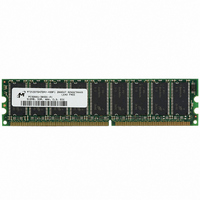
... ECC, SR), PC3200 184-Pin DDR SDRAM UDIMM MT9VDDT1672A – 128MB MT9VDDT3272A – 256MB MT9VDDT6472A – 512MB For the latest data sheet, please refer to the Micron site: www.micron.com/products/modules Figure 1: 184-Pin DIMM (MO-206) Standard 1.25in. (31.75mm) OPTIONS • Package 184-pin DIMM (standard) 184-pin DIMM (lead-free) • ...
Page 2
... DENSITY MT9VDDT1672AG-40B__ MT9VDDT1672AY-40B__ MT9VDDT3272AG-40B__ MT9VDDT3272AY-40B__ MT9VDDT6472AG-40B__ MT9VDDT6472AY-40B__ NOTE: All part numbers end with a two-place code (not shown), designating component and PCB revisions. Consult factory for current revision codes. Example: MT9VDDT3272AG-40BA1. pdf: 09005aef80a43e7d, source: 09005aef80a43d77 DDA9C16_32_64x72AG.fm - Rev. B 9/04 EN 128MB, 256MB, 512MB (x72, ECC, SR), PC3200 ...
Page 3
Table 3: Pin Assignment (184-Pin DIMM Front) PIN SYMBOL PIN SYMBOL PIN SYMBOL PIN SYMBOL DQ17 47 REF 2 DQ0 25 DQS2 DQ1 DQS0 ...
Page 4
Table 5: Pin Descriptions Pin numbers may not correlate with symbols; ; Refer to Pin Assignment Tables on page 3 for more information PIN NUMBERS SYMBOL 63, 65, 154 WE#, CAS#, RAS# 16, 17, 75, 76, 137, 138 CK0, CK0#, ...
Page 5
... This supply is isolated from the V NC – No Connects. DNU – Do Not Use: These pins are not connected on this module but are assigned pins on other modules in this product family. 5 184-Pin DDR SDRAM UDIMM / Micron Technology, Inc., reserves the right to change products or specifications without notice. ...
Page 6
... A0-A11 (128MB) A0-A12 (256MB, 512MB) NOTE: 1. All resistor values are 22 unless otherwise specified. 2. Per industry standard, Micron modules utilize various component speed grades, as referenced in the module part number guide at www.micron.com/numberguide. pdf: 09005aef80a43e7d, source: 09005aef80a43d77 DDA9C16_32_64x72AG.fm - Rev. B 9/04 EN 128MB, 256MB, 512MB (x72, ECC, SR), PC3200 ...
Page 7
... DDR SDRAM modules use internally configured quad-bank DDR SDRAM devices. DDR SDRAM modules use a double data rate archi- tecture to achieve high-speed operation. Double data rate architecture is essentially a 2n-prefetch architec- ture with an interface designed to transfer two data words per clock cycle at the I/O pins ...
Page 8
... Module BA1 BA0 M13 and M12 (BA0 and BA1) must be “0, 0” to select the base mode register (vs. the extended mode register). 256MB, 512MB Modules BA1 BA0 A12 A11 Operating Mode * M14 and M13 (BA0 and BA1) must be “0, 0” to select the base mode register (vs ...
Page 9
Table 6: Burst Definition Table ORDER OF ACCESSES WITHIN A STARTING BURST COLUMN TYPE = LENGTH ADDRESS SEQUENTIAL 0 0-1-2 1-2-3 2-3-0 3-0-1-2 A2 ...
Page 10
... READ command can be issued. pdf: 09005aef80a43e7d, source: 09005aef80a43d77 DDA9C16_32_64x72AG.fm - Rev. B 9/04 EN 128MB, 256MB, 512MB (x72, ECC, SR), PC3200 184-Pin DDR SDRAM UDIMM Figure 6: Extended Mode Register 128MB Module BA1 BA0 256MB, 512MB Modules BA1 BA0 A12 E12 E11 E10 E9 0 ...
Page 11
Commands Table 8, Commands Truth Table, and Table 9, DM Operation Truth Table, provide a general reference of available commands. For a more detailed description Table 8: Commands Truth Table DESELECT and NOP are functionally interchangeable; all states and sequences ...
Page 12
Absolute Maximum Ratings Stresses greater than those listed may cause perma- nent damage to the device. This is a stress rating only, and functional operation of the device at these or any other conditions above those indicated in the opera- ...
Page 13
Table 12: I Specifications and Conditions – 128MB DD DRAM components only Notes: 1–5, 8, 10, 12, 48; notes appear on pages 18–20; 0°C PARAMETER/CONDITION OPERATING CURRENT: One device bank; Active-Precharge (MIN (MIN); DQ, DM, ...
Page 14
Table 13: I Specifications and Conditions – 256MB DD DRAM components only Notes: 1–5, 8, 10, 12; notes appear on pages 18–20; 0°C PARAMETER/CONDITION OPERATING CURRENT: One device bank; Active-Precharge (MIN (MIN); DQ, DM, and ...
Page 15
Table 14: I Specifications and Conditions – 512MB DD DRAM components only Notes: 1–5, 8, 10, 12; notes appear on pages 18–20; 0°C PARAMETER/CONDITION OPERATING CURRENT: One device bank; Active-Precharge (MIN (MIN); DQ, DM, and ...
Page 16
Table 15: Capacitance Note: 11; notes appear on pages 18–20 PARAMETER Input/Output Capacitance: DQs, DQSs Input Capacitance: Command and Address, S0# Input Capacitance: CK, CK# Input Capacitance: CKE Table 16: DDR SDRAM Component Electrical Characteristics and Recommended AC Operating Conditions ...
Page 17
Table 16: DDR SDRAM Component Electrical Characteristics and Recommended AC Operating Conditions (Continued) Notes: 1–5, 8, 12–15, 29, 31; notes appear on page 18–20; 0°C AC CHARACTERISTICS PARAMETER ACTIVE to READ or WRITE delay PRECHARGE command period DQS read preamble ...
Page 18
Notes 1. All voltages referenced Tests for AC timing and electrical AC and DC DD characteristics may be conducted at nominal ref- erence/supply voltage levels, but the related spec- ifications and device operation are ...
Page 19
QHS). The data valid window derates in direct proportion to the clock duty cycle and a practical data valid window can be derived. The clock is allowed a maximum duty cycle variation ...
Page 20
... JEDEC operating frequency of 83 MHz. As such, future die may not reflect this option. pdf: 09005aef80a43e7d, source: 09005aef80a43d77 DDA9C16_32_64x72AG.fm - Rev. B 9/04 EN 128MB, 256MB, 512MB (x72, ECC, SR), PC3200 41. For -40B modules, I 42. Random addressing changing and 50 percent of 43. Random addressing changing and 100 percent of Q+1.5V for a pulse DD 44 ...
Page 21
Initialization To ensure device operation the DRAM must be ini- tialized as described below: 1. Simultaneously apply power Apply V and then V power. REF TT 3. Assert and hold CKE at a LVCMOS logic low. 4. ...
Page 22
SPD Clock and Data Conventions Data states on the SDA line can change only during SCL LOW. SDA state changes during SCL HIGH are reserved for indicating start and stop conditions (as shown in Figure 10, Data Validity, and Figure ...
Page 23
Table 17: EEPROM Device Select Code Most significant bit (b7) is sent first SELECT CODE Memory Area Select Code (two arrays) Protection Register Select Code Table 18: EEPROM Operating Modes MODE RW BIT Current Address Read Random Address Read Sequential ...
Page 24
Table 19: Serial Presence-Detect EEPROM DC Operating Conditions All voltages referenced DDSPD PARAMETER/CONDITION SUPPLY VOLTAGE INPUT HIGH VOLTAGE: Logic 1; All inputs INPUT LOW VOLTAGE: Logic 0; All inputs OUTPUT LOW VOLTAGE: IOUT = 3mA ...
Page 25
Table 21: Serial Presence-Detect Matrix “1”/“0”: Serial Data, “driven to HIGH”/“driven to LOW” BYTE DESCRIPTION 0 Number of SPD Bytes Used by Micron 1 Total Number of Bytes in SPD Device 2 Fundamental Memory Type 3 Number of Row Addresses ...
Page 26
Table 21: Serial Presence-Detect Matrix (Continued) “1”/“0”: Serial Data, “driven to HIGH”/“driven to LOW” BYTE DESCRIPTION 30 Minimum RAS# Pulse Width, 31 Module Rank Density 32 Address And Command Setup Time, 33 Address And Command Hold Time, 34 Data/ Data ...
Page 27
Figure 14: 184-Pin DIMM Dimensions 0.079 (2.00) R (4X 0.098 (2.50) D (2X) 0.091 (2.30) TYP. PIN 1 0.091 (2.30) 0.050 (1.27) TYP. TYP. PIN 184 1.95 (49.53) NOTE: All dimensions in inches (millimeters); Data Sheet Designation Released ...