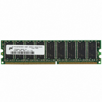
MT9VDDT6472AY-40BF1 Micron Technology Inc, MT9VDDT6472AY-40BF1 Datasheet - Page 13

MT9VDDT6472AY-40BF1
Manufacturer Part Number
MT9VDDT6472AY-40BF1
Description
MODULE DDR SDRAM 512MB 184-DIMM
Manufacturer
Micron Technology Inc
Datasheet
1.MT9VDDT6472AY-40BF1.pdf
(27 pages)
Specifications of MT9VDDT6472AY-40BF1
Memory Type
DDR SDRAM
Memory Size
512MB
Speed
400MT/s
Package / Case
184-DIMM
Lead Free Status / RoHS Status
Lead free / RoHS Compliant
Other names
557-1178
MT9VDDT6472AY-40BF1
MT9VDDT6472AY-40BF1
Table 12: I
DRAM components only
Notes: 1–5, 8, 10, 12, 48; notes appear on pages 18–20; 0°C
pdf: 09005aef80a43e7d, source: 09005aef80a43d77
DDA9C16_32_64x72AG.fm - Rev. B 9/04 EN
OPERATING CURRENT: One device bank; Active-Precharge;
(MIN);
clock cycle; Address and control inputs changing once every two clock
cycles;
OPERATING CURRENT: One device bank; Active-Read-Precharge;
Burst = 2;
control inputs changing once per clock cycle
PRECHARGE POWER-DOWN STANDBY CURRENT: All device banks idle;
Power-down mode;
IDLE STANDBY CURRENT: CS# = HIGH; All device banks idle;
(MIN); CKE = HIGH; Address and other control inputs changing once
per clock cycle. V
ACTIVE POWER-DOWN STANDBY CURRENT: One device bank active;
Power-down mode;
ACTIVE STANDBY CURRENT: CS# = HIGH; CKE = HIGH; One device
bank; Active-Precharge;
and DQS inputs changing twice per clock cycle; Address and other
control inputs changing once per clock cycle
OPERATING CURRENT: Burst = 2; Reads; Continuous burst; One device
bank active; Address and control inputs changing once per clock cycle;
t
OPERATING CURRENT: Burst = 2; Writes; Continuous burst; One device
bank active; Address and control inputs changing once per clock cycle;
t
cycle
AUTO REFRESH CURRENT
SELF REFRESH CURRENT: CKE
OPERATING CURRENT: Four device bank interleaving READs (BL = 4)
with auto precharge,
control inputs change only during Active, READ, or WRITE commands.
CK =
CK =
t
t
CK (MIN); I
CK (MIN); DQ, DM, and DQS inputs changing twice per clock
t
CK =
t
RC =
t
CK (MIN); DQ, DM, and DQS inputs changing once per
t
DD
RC (MIN);
IN
OUT
= V
t
t
Specifications and Conditions – 128MB
CK =
CK =
= 0mA
PARAMETER/CONDITION
t
RC =
REF
t
RC =
for DQ, DQS, and DM
t
t
t
CK (MIN); CKE = LOW;
CK (MIN); CKE = LOW
t
CK =
RC (MIN);
t
RAS (MAX);
0.2V
t
CK (MIN); I
t
CK =
128MB, 256MB, 512MB (x72, ECC, SR), PC3200
t
t
CK =
OUT
CK (MIN); Address and
t
t
Standard
REFC =
REFC = 15.625µs
= 0mA; Address and
t
CK (MIN); DQ, DM,
t
RFC (MIN)
t
RC =
13
t
T
CK =
A
t
+70°C; V
RC
t
CK
Micron Technology, Inc., reserves the right to change products or specifications without notice.
184-Pin DDR SDRAM UDIMM
SYMBOL
DD
I
I
I
I
I
I
I
DD 4 W
I
I
DD 3 N
DD 4 R
I
DD 5A
I
I
DD 2 P
DD 2 F
DD 3 P
DD 0
DD 1
DD 5
DD 6
DD 7
= V
DD
Q = +2.6V ±0.1V
MAX
1,035
1,215
1,215
1,395
2,160
3,195
-40B
450
225
450
27
54
36
UNITS
©2004 Micron Technology, Inc.
mA
mA
mA
mA
mA
mA
mA
mA
mA
mA
mA
mA
21, 28, 44
21, 28, 44
NOTES
20, 42
20, 42
20, 41
20, 42
20, 44
24, 44
20, 43
45
20
9


