H11A1SM Fairchild Optoelectronics Group, H11A1SM Datasheet - Page 2
H11A1SM
Manufacturer Part Number
H11A1SM
Description
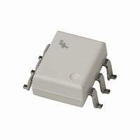
OPTOCOUPLER TRANS-OUT 6-SMD
Manufacturer
Fairchild Optoelectronics Group
Datasheet
1.H11A1SM.pdf
(9 pages)
Specifications of H11A1SM
Number Of Channels
1
Input Type
DC
Voltage - Isolation
7500Vpk
Current Transfer Ratio (min)
50% @ 10mA
Voltage - Output
30V
Current - Dc Forward (if)
60mA
Vce Saturation (max)
400mV
Output Type
Transistor with Base
Mounting Type
Surface Mount
Package / Case
6-SMD
Lead Free Status / RoHS Status
Lead free / RoHS Compliant
Current - Output / Channel
-
Current Transfer Ratio (max)
-
Other names
H11A1S-M
Available stocks
Company
Part Number
Manufacturer
Quantity
Price
Company:

Part Number:
H11A1SM
Manufacturer:
STM
Quantity:
2 000
Part Number:
H11A1SM
Manufacturer:
ON/安森美
Quantity:
20 000


©2005 Fairchild Semiconductor Corporation
4NXXM, H11AXM Rev. 1.0.2
Absolute Maximum Ratings
Stresses exceeding the absolute maximum ratings may damage the device. The device may not function or be
operable above the recommended operating conditions and stressing the parts to these levels is not recommended.
In addition, extended exposure to stresses above the recommended operating conditions may affect device reliability.
The absolute maximum ratings are stress ratings only.
Electrical Characteristics
Individual Component Characteristics
Isolation Characteristics
*Typical values at T
TOTAL DEVICE
EMITTER
DETECTOR
EMITTER
DETECTOR
Symbol
Symbol
Symbol
BV
BV
BV
I
T
V
V
V
T
T
F
R
C
I
I
V
C
OPR
P
V
P
P
CEO
CBO
STG
SOL
CEO
CBO
ECO
(pk)
V
I
I
ISO
ISO
ISO
F
CEO
CBO
ECO
CE
R
D
R
D
D
F
Storage Temperature
Operating Temperature
Wave solder temperature (see page 8 for reflow solder profile)
Total Device Power Dissipation @ T
DC/Average Forward Input Current
Reverse Input Voltage
Forward Current – Peak (300µs, 2% Duty Cycle)
LED Power Dissipation @ T
Collector-Emitter Voltage
Collector-Base Voltage
Emitter-Collector Voltage
Detector Power Dissipation @ T
Input Forward Voltage
Reverse Leakage Current
Collector-Emitter Breakdown Voltage
Collector-Base Breakdown Voltage
Emitter-Collector Breakdown Voltage
Collector-Emitter Dark Current
Collector-Base Dark Current
Capacitance
Characteristic
Input-Output Isolation Voltage
Isolation Resistance
Isolation Capacitance
Derate above 25°C
Derate above 25°C
Derate above 25°C
A
= 25°C
Parameter
(T
A
(T
= 25°C unless otherwise specified)
Parameter
A
A
= 25°C unless otherwise specified)
= 25°C
A
= 25°C
A
= 25°C
I
V
I
I
I
V
V
V
f = 60Hz, t = 1 sec
V
V
F
C
C
E
2
R
CE
CB
CE
I-O
I-O
Test Conditions
Test Conditions
= 10mA
= 100µA, I
= 1.0mA, I
= 100µA, I
= 6.0V
= 10V, I
= 10V
= 0V, f = 1 MHz
= 500 VDC
= &, f = 1MHz
F
F
F
F
= 0
= 0
= 0
= 0
Min. Typ.* Max.
7500
10
Min.
30
70
7
11
260 for 10 sec
-40 to +150
-40 to +100
Value
2.94
1.41
1.76
250
120
150
60
30
70
0.2
Typ.*
6
3
7
0.001
1.18
100
120
10
1
8
2
Max.
1.50
10
50
20
www.fairchildsemi.com
mW/°C
mW/°C
Units
Vac(pk)
Units
mW
mW
mW
mA
°C
°C
°C
V
A
V
V
V
pF
Unit
µA
nA
nA
pF
V
V
V
V
Related parts for H11A1SM
Image
Part Number
Description
Manufacturer
Datasheet
Request
R

Part Number:
Description:
OPTOCOUPLER TRANS-OUT 6-DIP
Manufacturer:
Fairchild Optoelectronics Group
Datasheet:

Part Number:
Description:
OPTOCOUPLER TRANS-OUT 6-SMD
Manufacturer:
Fairchild Optoelectronics Group
Datasheet:

Part Number:
Description:
LED 7-SEG SGL CC RED RHDP .3"
Manufacturer:
Fairchild Optoelectronics Group
Datasheet:

Part Number:
Description:
LED IR EMITTING 940NM SIDELOOKER
Manufacturer:
Fairchild Optoelectronics Group
Datasheet:
Part Number:
Description:
LED IR EMITTING GAAS 940NM 3MM
Manufacturer:
Fairchild Optoelectronics Group
Datasheet:
Part Number:
Description:
LED IR EMITTING ALGAAS 880NM 3MM
Manufacturer:
Fairchild Optoelectronics Group
Datasheet:
Part Number:
Description:
LED IR EMITTING 940NM SMD 2MM
Manufacturer:
Fairchild Optoelectronics Group
Datasheet:
Part Number:
Description:
IC PHOTOTRANS IR 940NM BLK 1.9MM
Manufacturer:
Fairchild Optoelectronics Group
Datasheet:
Part Number:
Description:
LED IR GAAS SIDELOOK 940NM
Manufacturer:
Fairchild Optoelectronics Group
Datasheet:
Part Number:
Description:
LED IR EMITTING 940NM 2MM SMD
Manufacturer:
Fairchild Optoelectronics Group
Datasheet:
Part Number:
Description:
LED 7-SEG SGL CC RED RHDP .3"
Manufacturer:
Fairchild Optoelectronics Group
Datasheet:

Part Number:
Description:
DIODE EMITTING GAAS IRED TO-46
Manufacturer:
Fairchild Optoelectronics Group
Datasheet:
Part Number:
Description:
DIODE EMITTING GAAS IRED TO-46
Manufacturer:
Fairchild Optoelectronics Group
Datasheet:

Part Number:
Description:
LED SS BIPO RED/GRN DIFF PCB 5MM
Manufacturer:
Fairchild Optoelectronics Group
Datasheet:

Part Number:
Description:
LED SS HI EFF GREEN DIFF 3MM
Manufacturer:
Fairchild Optoelectronics Group
Datasheet: