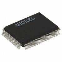
KS8993F Micrel Inc, KS8993F Datasheet - Page 44

KS8993F
Manufacturer Part Number
KS8993F
Description
IC CONV MED 10/100 3PORT 128PQFP
Manufacturer
Micrel Inc
Datasheet
1.KS8993F.pdf
(100 pages)
Specifications of KS8993F
Applications
*
Mounting Type
Surface Mount
Package / Case
128-MQFP, 128-PQFP
Number Of Primary Switch Ports
3
Internal Memory Buffer Size
32
Operating Supply Voltage (typ)
1.8/2.5/3.3V
Fiber Support
Yes
Integrated Led Drivers
Yes
Phy/transceiver Interface
MII/SNI
Power Supply Type
Analog/Digital
Package Type
PQFP
Data Rate (typ)
10/100Mbps
Vlan Support
Yes
Operating Temperature (max)
70C
Operating Temperature (min)
0C
Pin Count
128
Mounting
Surface Mount
Jtag Support
No
Operating Supply Voltage (max)
1.89/3.465V
Operating Temperature Classification
Commercial
Lead Free Status / RoHS Status
Lead free / RoHS Compliant
For Use With
KS8993F-EVAL - EVAL KIT EXPERIMENTAL KS8993F
Lead Free Status / RoHS Status
Not Compliant, Lead free / RoHS Compliant
Available stocks
Company
Part Number
Manufacturer
Quantity
Price
Part Number:
KS8993FA5
Manufacturer:
MICREL/麦瑞
Quantity:
20 000
Part Number:
KS8993FL
Manufacturer:
MICREL/麦瑞
Quantity:
20 000
Similarly, SPI multiple write is initiated when the master device continues to drive the KS8993F SPIS_N input pin low
after a byte (a register) is written. The KS8993F internal address counter will increment automatically to the next byte
(next register) after the write. The next byte that is sent from the master device to the KS8993F SDA input pin will be
written to the next register address. SPI multiple write will continue until the SPI master device terminates it by de-
asserting the SPIS_N signal to the KS8993F.
For both SPI multiple read and multiple write, the KS8993F internal address counter will wrap back to register address
zero once the highest register address is reached. This feature allows all 128 KS8993F registers to be read, or written
with a single SPI command and any initial register address.
The KS8993F is capable of supporting a 5 MHz SPI bus.
The following is a sample procedure for programming the KS8993F using the SPI bus:
Micrel, Inc.
June 2009
1. At the board level, connect the KS8993F pins as follows:
2. Enable SPI slave mode by setting the KS8993F strap-in pins PS[1:0] (pins 100 and 101 respectively) to “10”.
3. Power up the board and assert reset to the KS8993F. After reset, the “Start Switch” bit (register 1 bit 0) will be
4. Configure the desired register settings in the KS8993F, using the SPI write or multiple write command.
5. Read back and verify the register settings in the KS8993F, using the SPI read or multiple read command.
6. Write a ‘1’ to the “Start Switch” bit to start the KS8993F with the programmed settings.
set to ‘0’.
Note: The “Start Switch” bit cannot be set to ‘0’ to stop the switch after an ‘1’ is written to this bit. Thus, it is
recommended that all switch configuration settings are programmed before the “Start Switch” bit is set to ‘1’.
Some of the configuration settings, such as “Aging enable”, “Auto Negotiation Enable”, “Force Speed” and
“Power down” can be programmed after the switch has been started.
KS8993F
Pin #
99
97
98
96
Table 9: KS8993F SPI Connections
Signal Name
KS8993F
SPIS_N
(SPIC)
(SPID)
SPIQ
SDA
SCL
44
(Master output; Slave input)
(Master input; Slave output)
External Processor
Signal Description
SPI Slave Select
SPI Clock
SPI Data
SPI Data
hbwhelp@micrel.com
or (408) 955-1690
M9999-062509
KS8993F/FL


