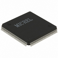
KS8695X Micrel Inc, KS8695X Datasheet - Page 21

KS8695X
Manufacturer Part Number
KS8695X
Description
IC SWITCH 10/100 5PORT 208PQFP
Manufacturer
Micrel Inc
Datasheet
1.KS8695X.pdf
(39 pages)
Specifications of KS8695X
Applications
*
Mounting Type
Surface Mount
Package / Case
208-MQFP, 208-PQFP
For Use With
KS8695-EVAL - EVAL KIT EXPERIMENTAL KS8695576-1005 - BOARD EVAL EXPERIMENT KS8695X
Lead Free Status / RoHS Status
Lead free / RoHS Compliant
Available stocks
Company
Part Number
Manufacturer
Quantity
Price
Reserved Pins
Advanced Memory Interface (SDRAM/ROM/FLASH/SRAM/EXTERNAL I/O)
Note:
1. I = Input.
October 2004
KS8695X
O = Output.
NC = No connect.
130
131
132
133
134
135
136
139
140
141
142
143
144
145
146
147
205
206
198
199
200
201
202
203
204
207
208
Pin
84
24
23
10
13
14
15
3
4
5
6
7
8
9
ADDR21/BA1
ADDR20/BA0
ADDR[19]
ADDR[18]
ADDR[17]
ADDR[16]
ADDR[15]
ADDR[14]
ADDR[13]
ADDR[12]
ADDR[11]
ADDR[10]
SDOCLK
ADDR[9]
ADDR[8]
ADDR[7]
ADDR[6]
ADDR[5]
ADDR[4]
ADDR[3]
ADDR[2]
ADDR[1]
ADDR[0]
TEST10
TEST11
TEST12
TEST13
TEST14
TEST15
TEST16
TEST17
TEST18
TEST19
SDICLK
TEST3
TEST4
TEST5
TEST6
TEST7
TEST8
TEST9
Name
I/O Type(
NC
NC
NC
NC
NC
NC
NC
NC
NC
NC
NC
NC
NC
NC
NC
NC
NC
O
O
O
O
I
1)
For SDRAM and ROM/SRAM/Flash, connect ADDR[0] to A0 on the memory,
ADDR[1] to A1 on the memory, and so forth. Address bit mapping for 8-bit,
16-bit, 32-bit access.
For external I/O devices, the system designer must connect address lines
conventionally for 8-bit, 16-bit, and 32-bit access.
Description
The Reserved Pins serve as no connect in order to ensure correct operation of
the device. DO NOT connect any signal to these pins.
No connect.
No connect.
No connect.
No connect.
No connect.
No connect.
No connect.
No connect.
No connect.
No connect.
No connect.
No connect.
No connect.
No connect.
No connect.
No connect.
SDRAM Clock In: SDRAM clock input for the SDRAM memory controller interface.
System/SDRAM Clock Out: Output of the internal system clock, it is also used as the
clock signal for SDRAM interface.
Address Bit 21/Bank Address Input 1: Address bit 21 for asynchronous accesses.
Bank Address Input bit 1 for SDRAM accesses.
Address Bit 20/Bank Address Input 0: Address bit 20 for asynchronous accesses.
Bank Address Input bit 0 for SDRAM accesses.
Address Bus: The 22-bit address bus (including ADDR[21:20] above) covers 4M word
memory space shared by ROM/SRAM/FLASH, SDRAM, and external I/O banks.
During the SDRAM cycles, the internal address bus is used to generate RAS and
CAS addresses for the SDRAM. The number of column address bits in the SDRAM
banks can be programmed from 8 to 11 bits via the SDRAM control registers.
ADDR[12:0] are the SDRAM address, and ADDR[21:20] are the SDRAM bank
address. During other cycles, the ADDR[21:0] is the byte address of the data transfer.
Note: The address pinout non-sequential by design. It is optimized for board level
connections to SDRAM.
21
M9999-102604
Micrel


