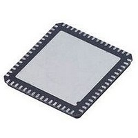
AD9267BCPZ Analog Devices Inc, AD9267BCPZ Datasheet - Page 8

AD9267BCPZ
Manufacturer Part Number
AD9267BCPZ
Description
IC MOD SIGMA-DELTA DUAL 64LFCSP
Manufacturer
Analog Devices Inc
Datasheet
1.AD9267BCPZRL7.pdf
(24 pages)
Specifications of AD9267BCPZ
Applications
*
Mounting Type
Surface Mount
Package / Case
64-LFCSP
Resolution (bits)
16bit
Sampling Rate
640MSPS
Input Channel Type
Differential
Data Interface
Serial, SPI
Supply Voltage Range - Analog
1.7V To 1.9V
Supply Voltage Range - Digital
1.7V To 1.9V
Lead Free Status / RoHS Status
Lead free / RoHS Compliant
AD9267
PIN CONFIGURATION AND FUNCTION DESCRIPTIONS
Table 7. Pin Function Descriptions
Pin No.
1
2
3, 4
5
6, 25, 43
7, 24, 42
8, 23, 41
9 to 16
17, 18
19, 20
21, 22, 26 to 30
31, 32
33 to 40
44, 45, 46
47
48
49
50
51, 62
52, 55, 58, 61
53, 54
56
57
59, 60
63
64
65
Mnemonic
CLK−
CVDD
PDWNA, PDWNB
PLL_LOCKED
DVDD
DGND
DRVDD
D0−B, D0+B to D3−B, D3+B
OR−B, OR+B
DCO−, DCO+
DNC
OR−A, OR+A
D0−A, D0+A to D3−A, D3+A
PLLMULT4, PLLMULT3, PLLMULT2
SDIO/PLLMULT1
SCLK/PLLMULT0
CSB
RESET
AGND
AVDD
VIN+A, VIN−A
VREF
CFILT
VIN+B, VIN−B
CGND
CLK+
Exposed paddle (EPAD)
PLL_LOCKED
NOTES
1. DNC = DO NOT CONNECT.
2. THE EXPOSED PAD MUST BE SOLDERED TO THE GROUND PLANE FOR THE
LFCSP PACKAGE. SOLDERING THE EXPOSED PADDLE TO THE PCB
INCREASES THE RELIABILITY OF THE SOLDER JOINTS, MAXIMIZING
THE THERMAL CAPACITY OF THE PACKAGE.
PDWNA
PDWNB
DRVDD
DGND
CVDD
DVDD
CLK–
D0–B
D0+B
D1–B
D1+B
D2–B
D2+B
D3–B
D3+B
10
12
13
14
15
16
11
1
2
3
4
5
6
7
8
9
Description
Differential Clock Input (−).
Clock Supply (1.8 V).
Power-Down Pins. Active high.
PLL Lock Indicator.
Digital Supply (1.8 V).
Digital Ground.
Digital Output Driver Supply
Channel B Differential LVDS Data Output Bits. D0+B is the LSB and D3+B is the MSB.
Channel B Overrange Indicator Pins.
Differential Data Clock Output.
Do Not Connect.
Channel A Overrange Indicator Pins.
Channel A Differential LVDS Data Output Bits. D0+A is the LSB and D3+A is the MSB.
PLL Mode Selection Pins.
Serial Port Interface Data Input/Output/PLL Mode Selection Pins.
Serial Port Interface Clock/PLL Mode Selection Pins.
Serial Port Interface Chip Select Pin Active Low.
Chip Reset.
Analog Ground.
Analog Supply (1.8 V).
Channel A Analog Input.
Voltage Reference Input.
Noise Limiting Filter Capacitor.
Channel B Analog Input.
Clock Ground.
Differential Clock Input (+).
Analog Ground. (Pin 65 is the exposed thermal pad on the bottom of the package.) The
exposed paddle must be soldered to analog ground of the PCB to achieve optimal electrical
and thermal performance.
PIN 1
INDICATOR
Figure 3. Pin Configuration
Rev. 0 | Page 8 of 24
(Not to Scale)
AD9267
TOP VIEW
48
47
46
45
44
43
42
41
40
39
38
37
36
35
34
33
SCLK/PLLMULT0
SDIO/PLLMULT1
PLLMULT2
PLLMULT3
PLLMULT4
DVDD
DGND
DRVDD
D3+A
D3–A
D2+A
D2–A
D1+A
D1–A
D0+A
D0–A


