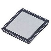
AD9267BCPZ Analog Devices Inc, AD9267BCPZ Datasheet - Page 14

AD9267BCPZ
Manufacturer Part Number
AD9267BCPZ
Description
IC MOD SIGMA-DELTA DUAL 64LFCSP
Manufacturer
Analog Devices Inc
Datasheet
1.AD9267BCPZRL7.pdf
(24 pages)
Specifications of AD9267BCPZ
Applications
*
Mounting Type
Surface Mount
Package / Case
64-LFCSP
Resolution (bits)
16bit
Sampling Rate
640MSPS
Input Channel Type
Differential
Data Interface
Serial, SPI
Supply Voltage Range - Analog
1.7V To 1.9V
Supply Voltage Range - Digital
1.7V To 1.9V
Lead Free Status / RoHS Status
Lead free / RoHS Compliant
AD9267
Differential Input Configurations
Optimum performance can be achieved by driving the AD9267
in a differential input configuration. The ADA4937-2 differential
driver provides excellent performance and a flexible interface to
the ADC. The output common-mode voltage of the ADA4937-2 is
easily set by connecting AVDD to the V
(see Figure 33). The noise and linearity of the ADA4937-2 needs
important consideration because the system performance may
be limited by the ADA4937-2.
For frequencies offset from dc, where SNR is a key parameter,
differential transformer coupling is the recommended input
configuration. An example is shown in Figure 34. The center
tap of the secondary winding of the transformer is connected to
AVDD to bias the analog input.
The signal characteristics must be considered when selecting a
transformer. Most RF transformers saturate at frequencies
below a couple of megahertz (MHz), and excessive signal power
can cause core saturation, which leads to distortion.
Voltage Reference
A stable and accurate 0.5 V voltage reference is built into the
AD9267. The reference voltage should be decoupled to minim-
ize the noise bandwidth using a 10 μF capacitor. The reference
is used to generate a bias current into a matched resistor such
that when used to bias the current in the feedback DAC, a
voltage of AVDD − 0.5 V is developed at the internal side of the
input resistors (see Figure 35). The current bias circuit should
also be decoupled on the CFILT pin with a 10 μF capacitor. For
this reason, the VREF voltage should always be 0.5 V.
V
50Ω
Figure 33. Differential Input Configuration Using the ADA4937-2
SOURCE
S
SIGNAL
49.9Ω
0.1µF
V
50Ω
SOURCE
S
SIGNAL
Figure 34. Differential Transformer Configuration
2V p-p
R
60.4
T
60.4Ω
V
2V p-p
OCM2
200Ω
0.1µF
R
50Ω
T
11
6
7
0.1µF
ADA4937-2
1:1
15
+5V
–5V
9
200Ω
200Ω
12
0.1µF
13
VIN+x
VIN–x
OCMx
VIN–x
VIN+x
pin of the ADA4937-2
AD9267
AVDD
AD9267
AVDD
+1.8V
0.1µF
Rev. 0 | Page 14 of 24
0.5V
Internal Reference Connection
To minimize thermal noise, the internal reference on the AD9267
is an unbuffered 0.5 V. It has an internal 10 kΩ series resistor,
which, when externally decoupled with a 10 μF capacitor, limits
the noise (see Figure 36). Do not use the unbuffered reference
to drive any external circuitry. The internal reference is used by
default and when Serial Register 0x18[6] is reset.
External Reference Operation
If an external reference is desired, the internal reference can be
disabled by setting Serial Register 0x18[6] high. Figure 37 shows
an application using the ADR130B as a stable external reference.
CLOCK INPUT CONSIDERATIONS
The AD9267 offers two modes of sourcing the ADC sample
clock (CLK+ and CLK−). The first mode uses an on-chip clock
multiplier that accepts a reference clock operating at the lower
input frequency. The on-chip phase-locked loop (PLL) then
multiplies the reference clock up to a higher frequency, which is
then used to generate all the internal clocks required by the Σ-Δ
modulator.
The clock multiplier provides a high quality clock that meets
the performance requirements of most applications. Using the
on-chip clock multiplier removes the burden of generating and
distributing the high speed clock.
10µF
VREF
AVDD
10kΩ
10µF
10µF
0.1µF
Figure 37. External Reference Configuration
Figure 36. Internal Reference Configuration
V IN p-p = 2V
V
TO CURRENT
CM
GENERATOR
CFILT
Figure 35. Voltage Reference Loop
AVDD – 0.5V
ADR130B
= AVDD
10kΩ
REF
VIN+x
VIN–x
0.5V
AVDD
10µF
500Ω
500Ω
500Ω
0.5V
2.85kΩ
AVDD – 0.5V
3.5kΩ
10kΩ
TO CURRENT
GENERATOR
8.5kΩ
TO LOOP
STAGE 2
FILTER


