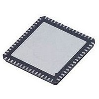
AD9267BCPZ Analog Devices Inc, AD9267BCPZ Datasheet - Page 18

AD9267BCPZ
Manufacturer Part Number
AD9267BCPZ
Description
IC MOD SIGMA-DELTA DUAL 64LFCSP
Manufacturer
Analog Devices Inc
Datasheet
1.AD9267BCPZRL7.pdf
(24 pages)
Specifications of AD9267BCPZ
Applications
*
Mounting Type
Surface Mount
Package / Case
64-LFCSP
Resolution (bits)
16bit
Sampling Rate
640MSPS
Input Channel Type
Differential
Data Interface
Serial, SPI
Supply Voltage Range - Analog
1.7V To 1.9V
Supply Voltage Range - Digital
1.7V To 1.9V
Lead Free Status / RoHS Status
Lead free / RoHS Compliant
AD9267
In normal operation mode, the analog input can toggle the
OR±x pin for a number of clock cycles as it approaches full
scale. The OR±x pin is a pulse-width modulated (PWM) signal;
therefore, as the analog input increases in amplitude, the
duration of OR±x pin toggling increases. Eventually, when the
OR±x pin is high for an extended period of time, the ADC
overloads; thus, there is little correspondence between analog
input and digital output. In this mode, the duration of the
OR±x pin can be used as a coarse indicator to the signal
amplitude at the input of the ADC. In data valid mode, the
OR±x pin remains high when there are no memory access
operations taking place, such as internal calibration or factory
memory transfer, and the inputs of the ADC are within the
operating range.
In either modes of operation, the AUTORST bit can be enabled
and this automatically resets the modulator in an overload
condition. Because the OR±x signal is a PWM signal and the
toggling of OR±x does not always indicate an overload
condition, the modulator only resets after 16 consecutive clock
Table 12. OR±x Conditions
Reset State
Normal Reset Off
Data Valid Reset Off
Normal Reset On
Data Valid Reset On
AUTORST
0
0
1
1
OR_IND1
0
1
0
1
OR_IND2
0
1
0
1
Rev. 0 | Page 18 of 24
cycles where OR±x remains high or if the loop filter becomes
saturated. The OR±x pin remains high until the automatic reset
has completed.
If the AD9267 is used in a system that incorporates automatic
gain control (AGC), the OR±x signals can be used to indicate
that the signal amplitude should be reduced. This may be
particularly effective for use in maximizing the signal dynamic
range if the signal includes high occurrence components that
occasionally exceed full scale by a small amount.
TIMING
The AD9267 provides latched data outputs with a latency of
seven clock cycles. The AD9267 also provides a data clock
output (DCO±) pin intended to assist in capturing the data in
an external register. The data outputs are valid on the rising
edge of DCO±, unless changed by setting Serial Register 0x16[7]
(see the Serial Port Interface (SPI) section). See Figure 2 for a
graphical timing description.
If overrange: OR±x = 1, else OR±x = 0
If memory access: OR±x = 0, else OR±x = 1
If overrange or reset: OR±x = 1, else OR±x = 0
Function
If memory access, or reset: OR±x = 0, else OR±x = 1


