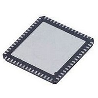
AD9267BCPZ Analog Devices Inc, AD9267BCPZ Datasheet - Page 16

AD9267BCPZ
Manufacturer Part Number
AD9267BCPZ
Description
IC MOD SIGMA-DELTA DUAL 64LFCSP
Manufacturer
Analog Devices Inc
Datasheet
1.AD9267BCPZRL7.pdf
(24 pages)
Specifications of AD9267BCPZ
Applications
*
Mounting Type
Surface Mount
Package / Case
64-LFCSP
Resolution (bits)
16bit
Sampling Rate
640MSPS
Input Channel Type
Differential
Data Interface
Serial, SPI
Supply Voltage Range - Analog
1.7V To 1.9V
Supply Voltage Range - Digital
1.7V To 1.9V
Lead Free Status / RoHS Status
Lead free / RoHS Compliant
AD9267
The reference clock, CLK±, is limited to 30 MHz to 160 MHz
when configured to use the on-chip clock multiplier. Given the
input range of the reference clock and the available multiplica-
tion factors, the f
the desired f
The PLL of the AD9267 can be controlled through either the serial
port interface or the PLLMULTx pins. For serial port interface
control, Register 0x09 and Register 0x0A are used. Before the
PLL enable register bit (PLLENABLE) is set, the PLL multiplica-
tion factor should be programmed into Register 0x0A[5:0].
After setting the PLLENABLE bit, the PLL locks and reports a
locked state in Register 0x0A[7]. If the PLL multiplication factor
is changed, the PLL enable bit should be reset and set again.
Some common clock multiplication factors are shown in Table 8.
The recommended sequence for enabling and programming the
on-chip clock multiplier is as follows:
1.
2.
3.
External PLL Control
At power-up, the serial interface is disabled until the first serial
port access. If the serial interface is disabled, the PLLMULTx
pins control the PLL multiplication factor. The five PLLMULTx
pins (Pin 44 to Pin 48) offer all the available multiplication
factors. If all PLLMULTx pins are tied high, the PLL is disabled
and the AD9267 assumes the high frequency modulator clock
rate that is applied to the CLK± pins. Table 10 shows the relation-
ship between PLLMULTx pins and the PLL multiplication factor.
PLL Autoband Select
The PLL VCO has a wide operating range that is covered by
overlapping frequency bands. For any desired VCO output fre-
quency, there are multiple valid PLL band select values. The
AD9267 possesses an automatic PLL band select feature on chip
that determines the optimal PLL band setting. This feature can
be enabled by writing to Register 0x0A[6] and is the recom-
mended configuration with the PLL clocking option.
Apply a reference clock to the CLK± pins.
Program the PLL multiplication factor in
Register 0x0A[5:0]. See Table 8.
Enable the PLL; Register 0x09 = 04 (decimal).
MOD
rate of 640 MHz with a 50% duty cycle.
VCO
is approximately 1280 MHz. This results in
Rev. 0 | Page 16 of 24
Table 8. PLL Multiplication Factors
0x0A[5:0]
1
2
3
4
5
6
7
8
9
10
11
12
13
14
15
16
17
18
19
20
21
22
23
24
25
26
27
28
29
30
31
32
Table 9. Common Modulator Clock Multiplication Factors
CLK±
(MHz)
30.72
39.3216
52.00
61.44
76.80
78.00
78.6432
89.60
92.16
122.88
134.40
153.60
157.2864
0x0A[5:0]
(PLLMULT)
42
32
25
21
17
17
16
15
14
10
10
8
8
PLLMULT (N)
8
8
8
8
8
8
8
8
9
10
10
12
12
14
15
16
17
18
18
20
21
21
21
24
25
25
25
28
28
30
30
32
f
(MHz)
1290.24
1258.29
1300.00
1290.24
1305.60
1326.00
1258.29
1344.00
1290.24
1228.80
1344.00
1228.80
1258.29
VCO
0x0A[5:0]
33
34
35
36
37
38
39
40
41
42
43
44
45
46
47
48
49
50
51
52
53
54
55
56
57
58
59
60
61
62
63
64
f
(MHz)
645.12
629.15
650.00
645.12
652.80
663.00
629.15
672.00
645.12
614.40
672.00
614.40
629.15
MOD
PLLMULT (N)
32
34
34
34
34
34
34
34
34
42
42
42
42
42
42
42
42
42
42
42
42
42
42
42
42
42
42
42
42
42
42
42
BW
(MHz)
10.08
9.83
10.16
10.08
10.20
10.36
9.83
10.50
10.08
9.60
10.50
9.60
9.83


