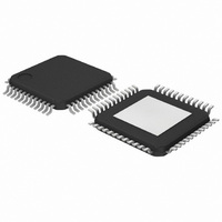
TZA1038HW,118 NXP Semiconductors, TZA1038HW,118 Datasheet - Page 38

TZA1038HW,118
Manufacturer Part Number
TZA1038HW,118
Description
IC DVD SIGNAL PROC 48-HTQFP
Manufacturer
NXP Semiconductors
Datasheet
1.TZA1038HW118.pdf
(45 pages)
Specifications of TZA1038HW,118
Applications
*
Mounting Type
Surface Mount
Package / Case
48-TQFP Exposed Pad, 48-eTQFP, 48-HTQFP, 48-VQFP
Lead Free Status / RoHS Status
Lead free / RoHS Compliant
Other names
935273843118
TZA1038HW-T
TZA1038HW-T
TZA1038HW-T
TZA1038HW-T
Available stocks
Company
Part Number
Manufacturer
Quantity
Price
Company:
Part Number:
TZA1038HW,118
Manufacturer:
NXP Semiconductors
Quantity:
10 000
Philips Semiconductors
11 APPLICATION INFORMATION
11.1
Simplified relationships between signals are described in
this section. In the simplification, all built-in options for
DVD-ROM are omitted. The variables A
A
G
11.1.1
Pins RFP and RFN carry the RF data signals in opposite
phases with respect to each other. This allows an ADC
with a balanced or differential input to be used in the
decoder. Depending on the DC input ranges of the ADC,
in many cases the connection between TZA1038HW and
the decoder can be a DC pin to pin connection. The
common mode DC level of pins RFP and RFN can be
chosen independently by means of input pin RFREF.
If bit RFSUM = 0
If bit RFSUM = 1
Where:
Correct settings for V
keep both V
specified for the TZA1038HW and the decoder.
2003 Sep 03
LFR
LFR
V
V
V
V
MN
V
MN
V
A
V
the voltage at pin OPUREF
V
(register 4 and register 5)
V
High speed advanced analog DVD signal
processor and laser supply
RFP
RFN
RFDIF
RFP
RFN
RFDIF
1
I
RFOFFS
RFREF
, are the linear equivalents of bits G
, A
= average input voltage at pins A to D, with respect to
.
Signal relationships
V
V
2
= V
= V
= V
= V
, A
RFOFFSS
RFOFFSS
D
= A
= A
is the input voltage at pin RFREF.
ATA PATH
RFREF
RFREF
3
is the programmed RF
RFREF
RFREF
RFP
and A
3
RFSUM
and V
A
)
)
+ 0.5
+ 0.5
2
RFSUM
0.5
0.5
A
A
RFREF
RFN
1
3
(V
A
A
A
A
are programmed gain values
at the DC voltage levels
(V
RFSUM
RFSUMP
RFSUM
3
3
and V
I
A
A
V
2
2
RFOFFS
RFOFFS
OFFS
A
A
A
A
V
1
1
3
3
RFSUMN
DAC voltage
1
).
1
(V
(V
(V
(V
are required to
to A
to G
I
I
RFSUMP
RFSUMP
V
V
3
3
, A
, G
RFOFFS
RFOFFS
V
RFOFFSS
LFC
LFC
V
V
and
and
RFSU
RFSU
)
)
).
38
11.1.2
The current through output pins OA to OD represents the
low-pass filtered input voltage of each individual pick-up
segment. The gain from input to output can be
programmed to adapt to different disc types or pick-ups
(offset cancellation is omitted for simplicity):
or:
or:
Where:
Phase difference =
180 <
A
and radial paths
Gain should be programmed such that maximum signal
levels fit into the range of the servo processor ADC
V
at pins A to D with respect to pin OPUREF
I
I
I
I
I
I
I
I
I
DC
FS
Ox
S1
S2
S1
S2
S1
S2
LFC
I(A)
is the sensitivity to relative phase difference.
is a DC current that keeps I
=
=
=
=
=
=
; V
=
and A
---------------------------------------------------- -
---------------------------------------------------- -
V
----------------------------- -
V
----------------------------- -
I
I
S
V
-------------------------- -
I(B)
DC
DC
V
V
< + 180 .
ERVO PATH
I(E)
I(F)
Ix
14 k
I(A)
I(C)
15 k
15 k
; V
+
–
LFR
I
A
I
+
+
I(C)
FS
FS
A
A
30 k
30 k
LFC
V
V
LFR
LFR
are the programmable gains in central
I(B)
I(D)
and V
phase difference
phase difference
----- -
T
p
(in CD three-beam push-pull mode)
(in CD three-beam push-pull mode)
t
=
A
I(D)
A
LFR
--------------------------------- -
LFR
are defined as input voltages
degrees
(in DVD push-pull mode)
(in DVD push-pull mode)
360
S1
TZA1038HW
and I
Product specification
(in DPD mode)
(in DPD mode)
;
S2
unipolar


