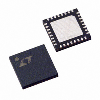
LTC3731CUH Linear Technology, LTC3731CUH Datasheet - Page 25

LTC3731CUH
Manufacturer Part Number
LTC3731CUH
Description
IC SW REG CTRLR SYNC BUCK 32QFN
Manufacturer
Linear Technology
Series
PolyPhase®r
Type
Step-Down (Buck)r
Datasheet
1.LTC3731CUHPBF.pdf
(32 pages)
Specifications of LTC3731CUH
Internal Switch(s)
No
Synchronous Rectifier
Yes
Number Of Outputs
1
Voltage - Output
0.6 ~ 6 V
Frequency - Switching
225kHz ~ 680kHz
Voltage - Input
4 ~ 36 V
Operating Temperature
0°C ~ 70°C
Mounting Type
Surface Mount
Package / Case
32-QFN
Lead Free Status / RoHS Status
Contains lead / RoHS non-compliant
Current - Output
-
Power - Output
-
Available stocks
Company
Part Number
Manufacturer
Quantity
Price
Company:
Part Number:
LTC3731CUH
Manufacturer:
Linear Technology
Quantity:
135
Company:
Part Number:
LTC3731CUH
Manufacturer:
LT
Quantity:
10 000
Part Number:
LTC3731CUH
Manufacturer:
LINEAR/凌特
Quantity:
20 000
Part Number:
LTC3731CUH#PBF
Manufacturer:
LINEAR/凌特
Quantity:
20 000
Part Number:
LTC3731CUH#TRPBF
Manufacturer:
LINEAR/凌特
Quantity:
20 000
APPLICATIO S I FOR ATIO
Simplified Visual Explanation of How a 3-Phase
Controller Reduces Both Input and Output RMS
Ripple Current
The effect of multiphase power supply design significantly
reduces the amount of ripple current in both the input and
output capacitors. The RMS input ripple current is divided
by, and the effective ripple frequency is multiplied up by
the number of phases used (assuming that the input
voltage is greater than the number of phases used times
the output voltage). The output ripple amplitude is also
reduced by, and the effective ripple frequency is increased
by the number of phases used. Figure 13 graphically
illustrates the principle.
The worst-case input RMS ripple current for a single stage
design peaks at twice the value of the output voltage. The
worst-case input RMS ripple current for a two stage
design results in peaks at 1/4 and 3/4 of the input voltage,
and the worst-case input RMS ripple current for a three
stage design results in peaks at 1/6, 1/2, and 5/6 of the
input voltage. The peaks, however, are at ever decreasing
U
U
W
Figure 13. Single and PolyPhase Current Waveforms
I
I
V
V
V
COUT
COUT
V
SW1
SW2
SW3
I
I
CIN
CIN
SW
I
I
I
L1
L2
L3
U
SINGLE PHASE
TRIPLE PHASE
levels with the addition of more phases. A higher effective
duty factor results because the duty factors “add” as long
as the currents in each stage are balanced. Refer to AN19
for a detailed description of how to calculate RMS current
for the single stage switching regulator.
Figure 6 illustrates the RMS input current drawn from the
input capacitance versus the duty cycle as determined by
the ratio of input and output voltage. The peak input RMS
current level of the single phase system is reduced by 2/3
in a 3-phase solution due to the current splitting between
the three stages.
The output ripple current is reduced significantly when
compared to the single phase solution using the same
inductance value because the V
term from the stages that has their bottom MOSFETs on
subtract current from the (V
resulting from the stage which has its top MOSFET on. The
output ripple current for a 3-phase design is:
I
P-P
=
3731 F13
( )( )
V
f L
OUT
(
1 3
–
DC
)
CC
V
IN
– V
>
OUT
OUT
3
V
/L discharge currents
OUT
)/L charging current
LTC3731
25
3731fb


