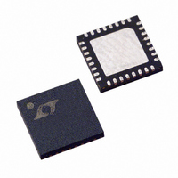
LTC3731CUH Linear Technology, LTC3731CUH Datasheet - Page 17

LTC3731CUH
Manufacturer Part Number
LTC3731CUH
Description
IC SW REG CTRLR SYNC BUCK 32QFN
Manufacturer
Linear Technology
Series
PolyPhase®r
Type
Step-Down (Buck)r
Datasheet
1.LTC3731CUHPBF.pdf
(32 pages)
Specifications of LTC3731CUH
Internal Switch(s)
No
Synchronous Rectifier
Yes
Number Of Outputs
1
Voltage - Output
0.6 ~ 6 V
Frequency - Switching
225kHz ~ 680kHz
Voltage - Input
4 ~ 36 V
Operating Temperature
0°C ~ 70°C
Mounting Type
Surface Mount
Package / Case
32-QFN
Lead Free Status / RoHS Status
Contains lead / RoHS non-compliant
Current - Output
-
Power - Output
-
Available stocks
Company
Part Number
Manufacturer
Quantity
Price
Company:
Part Number:
LTC3731CUH
Manufacturer:
Linear Technology
Quantity:
135
Company:
Part Number:
LTC3731CUH
Manufacturer:
LT
Quantity:
10 000
Part Number:
LTC3731CUH
Manufacturer:
LINEAR/凌特
Quantity:
20 000
Part Number:
LTC3731CUH#PBF
Manufacturer:
LINEAR/凌特
Quantity:
20 000
Part Number:
LTC3731CUH#TRPBF
Manufacturer:
LINEAR/凌特
Quantity:
20 000
APPLICATIO S I FOR ATIO
special polymer capacitors available in case heights
ranging from 2mm to 4mm. Other capacitor types in-
clude Sanyo POSCAP, Sanyo OS-CON, Nichicon PL
series and Sprague 595D series. Consult the manufac-
turers for other specific recommendations.
R
Once the frequency and inductor have been chosen,
R
required peak inductor current. The current comparator
has a typical maximum threshold of 75mV/R
input common mode range of SGND to (1.1) • V
current comparator threshold sets the peak inductor cur-
rent, yielding a maximum average output current I
equal to the peak value less half the peak-to-peak ripple
current, ∆I
Allowing a margin for variations in the IC and external
component values yields:
The IC works well with values of R
to 0.02Ω.
V
The V
of the controller but also to the top and bottom gate
drivers in the LTC3731 UH package, and therefore must
be bypassed very carefully to ground with a ceramic
capacitor, type X7R or X5R (depending upon the operat-
ing temperature environment) of at least 1 µ F imme diately
next to the IC and preferably an additional 10µF placed very
close to the IC due to the extremely high instantaneous
currents involved. The total capacitance, taking into ac-
count the voltage coefficient of ceramic capacitors, should
be 100 times as large as the total combined gate charge
capacitance of ALL of the MOSFETs being driven. Good
bypassing close to the IC is necessary to supply the high
transient currents required by the MOSFET gate drivers
while keeping the 5V supply quiet enough so as not to
disturb the very small-signal high bandwidth of the cur-
rent comparators.
CC
SENSE
SENSE1,
R
Decoupling
SENSE
CC
Selection for Output Current
pin supplies power not only to the internal circuits
R
L
SENSE2,
=
.
N
50
I
MAX
mV
R
U
SENSE3
U
are determined based on the
W
SENSE
from 0.002Ω
SENSE
U
CC
and an
. The
MAX
Topside MOSFET Driver Supply (C
External bootstrap capacitors, C
BOOST pins, supply the gate drive voltages for the
topside MOSFETs. Capacitor C
gram is charged though diode D
SW pin is low. When one of the topside MOSFETs turns
on, the driver places the C
source of the desired MOSFET. This enhances the
MOSFET and turns on the topside switch. The switch
node voltage, SW, rises to V
follows. With the topside MOSFET on, the boost voltage
is above the input supply (V
value of the boost capacitor C
times that of the total gate charge capacitance of the
topside MOSFET(s) as specified on the manufacturer’s
data sheet. The reverse breakdown of D
greater than V
Differential Amplifier/Output Voltage Programming
The IC has a true remote voltage sense capability. The
sensing connections should be returned from the load,
back to the differential amplifier’s inputs through a com-
mon, tightly coupled pair of PC traces. The differential
amplifier rejects common mode signals capacitively or
inductively radiated into the feedback PC traces as well as
ground loop disturbances. The differential amplifier out-
put signal is divided down with an external resistive divider
and compared with the internal, precision 0.6V voltage
reference by the error amplifier.
The differential amplifier has a 0V to V
input range and an output swing range of 0V to V
The output uses an NPN emitter follower without any
internal pull-down current. A DC resistive load to ground
is required in order to sink current.
The output voltage is set by an external resistive divider
according to the following formula:
The resistive divider is connected to the output as shown
in Figure 2, allowing remote voltage sensing.
V
OUT
=
0 6 1
.
V
IN(MAX).
⎛
⎜
⎝
+
R
R
2
1
⎞
⎟
⎠
B
voltage across the gate-
BOOST
B
B
IN
needs to be 30 to 100
in the Functional Dia-
B
B
and the BOOST pin
B
, connected to the
, D
from V
= V
CC
B
)
LTC3731
CC
common mode
CC
+ V
B
when the
CC
must be
IN
17
– 1.2V.
). The
3731fb


