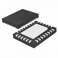
LTC3546IUFD#PBF Linear Technology, LTC3546IUFD#PBF Datasheet - Page 4

LTC3546IUFD#PBF
Manufacturer Part Number
LTC3546IUFD#PBF
Description
IC BUCK SYNC ADJ 1A/2A DL 28QFN
Manufacturer
Linear Technology
Type
Step-Down (Buck)r
Datasheet
1.LTC3546EUFDTRPBF.pdf
(28 pages)
Specifications of LTC3546IUFD#PBF
Internal Switch(s)
Yes
Synchronous Rectifier
Yes
Number Of Outputs
2
Voltage - Output
0.6 ~ 5 V
Current - Output
1A, 2A
Frequency - Switching
2.25MHz, 0.75MHz ~ 4MHz
Voltage - Input
2.25 ~ 5.5 V
Operating Temperature
-40°C ~ 125°C
Mounting Type
Surface Mount
Package / Case
28-QFN
Dc To Dc Converter Type
Step Down
Pin Count
28
Input Voltage
5.5V
Output Voltage
0.6 to 5V
Switching Freq
750 TO 4000/2900KHz
Output Current
2A
Efficiency
96%
Package Type
QFN EP
Output Type
Adjustable
Switching Regulator
Yes
Load Regulation
0.2%
Line Regulation
0.2%/V
Mounting
Surface Mount
Input Voltage (min)
2.25V
Operating Temperature Classification
Automotive
Lead Free Status / RoHS Status
Lead free / RoHS Compliant
Power - Output
-
Lead Free Status / Rohs Status
Compliant
Available stocks
Company
Part Number
Manufacturer
Quantity
Price
ELECTRICAL CHARACTERISTICS
LTC3546
junction temperature range, otherwise specifi cations are at T
SYMBOL
I
I
V
T
T
R
R
t
V
V
I
I
VTL
VTH
V
I
VTH
I
Note 1: Stresses beyond those listed under Absolute Maximum Ratings
may cause permanent damage to the device. Exposure to any Absolute
Maximum Rating condition for extended periods may affect device
reliability and lifetime.
Note 2: The LTC3546E is guaranteed to meet performance specifi cations
from 0°C to 85°C. Specifi cations over the –40°C to 125°C operating
junction temperature range are assured by design, characterization and
correlation with statistical process controls. The LTC3546I is guaranteed
to meet performance specifi cations over the full –40°C to 125°C operating
junction temperature range
Note 3: The LTC3546 is tested in feedback loop which servos V
midpoint for the error amplifi er (V
the error amplifi er (V
Note 4: Total supply current is higher due to the internal gate charge being
delivered at the switching frequency.
4
SW1D(LKG)
SW2A/B(LKG)
SS
RUN1
PHASE
SYNC/MODE
BMC1
PGOOD1
PGOOD2
UVLO
RUN1
PHASE
SYNC/MODE
PGOOD1
PGOOD2
SYNC/MODE
SYNC/MODE
FREQ
, I
, I
, V
RUN2
BMC2
RUN2
,
,
PARAMETER
Switch Leakage Current SW1D
Switch Leakage Current SW2A/B
Undervoltage Lockout Threshold
Threshold for Power Good
Percentage Deviation from Regulated V
(Typically 0.6V).
Threshold for Power Good
Percentage Deviation from Regulated V
(Typically 0.6V).
Power Good Pull-Down On-Resistance
Power Good Pull-Down On-Resistance
Soft-Start Internal Time.
RUN1, RUN2, and PHASE Threshold
RUN1, RUN2, and PHASE Leakage Current V
SYNC/MODE Threshold Voltage Low to Put
the Part into Pulse-Skipping Mode
SYNC/MODE Threshold Voltage High to
Put the Part into Burst Mode Operation
SYNC/MODE Threshold for Clock
Synchronization
SYNC/MODE Leakage Current
FREQ Threshold Voltage High
BMC1, BMC2 Leakage Current
ITH2
= 0.6V).
ITH1
= 0.6V) and V
FB2
FB1
FB2
to the midpoint for
CONDITIONS
V
V
V
V
V
V
V
V
V
V
V
V
V
FB1
IN
ITH1
RUN1
IN
ITH2
RUN2
IN1
IN1
FB1
FB2
FB
IN
IN
IN
= 6V
= 6V
= 6V, V
= 6V, V
= 6V, V
from 0% to 95%, V
, V
, V
to the
Ramping Up, V
Ramping Up, V
The
= V
= 0V
= V
= 0V
IN2
IN2
A
ITH2
, V
, V
RUN2
= 25°C. V
PHASE
SYNC/MODE
BMC
l
CCA
CCA
denotes the specifi cations which apply over the full operating
= 0V
= 3V
= 0V
, V
, V
= 3V, V
Note 5: Variable frequency operation with resistor is guaranteed by design
and is subject to duty cycle limitations.
Note 6: This IC includes overtemperature protection that is intended
to protect the device during momentary overload conditions. Junction
temperature will exceed 125°C when overtemperature protection is active.
Continuous operation above the specifi ed maximum operating junction
temperature may impair device reliability.
Note 7: T
dissipation, P
Note 8: Minimum current limit is guaranteed by design and correlation to
the R
CCD
CCD
SYNC/MODE
SYNC/MODE
IN
= 3V
T
Rising
Falling
J
TRACK/SS
RUN1
DS(ON)1D
= V
= T
CCA
J
A
= V
is calculated from the ambient temperature, T
+ (P
= 0V
= 0V
D
= 3.6V, unless otherwise specifi ed. (Note 2)
, I
Is Floating
RUN2
, according to the following formula:
D
LIM1
• 34°C/W)
= 3V
and I
LIM2
measurements.
V
V
IN
IN
2.03
1.86
MIN
0.8
0.3
0.3
– 0.85
– 0.5
±0.01
±0.01
0.01
0.01
2.14
1.97
TYP
132
132
1.2
0.8
0.8
–8
–8
A
, and power
MAX
2.03
±0.4
300
300
2.2
1.9
1.2
0.5
1.2
±1
±1
1
1
UNITS
3546fb
ms
μA
μA
μA
μA
μA
%
%
Ω
Ω
V
V
V
V
V
V
V


