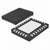
LTC3546IUFD#PBF Linear Technology, LTC3546IUFD#PBF Datasheet - Page 10

LTC3546IUFD#PBF
Manufacturer Part Number
LTC3546IUFD#PBF
Description
IC BUCK SYNC ADJ 1A/2A DL 28QFN
Manufacturer
Linear Technology
Type
Step-Down (Buck)r
Datasheet
1.LTC3546EUFDTRPBF.pdf
(28 pages)
Specifications of LTC3546IUFD#PBF
Internal Switch(s)
Yes
Synchronous Rectifier
Yes
Number Of Outputs
2
Voltage - Output
0.6 ~ 5 V
Current - Output
1A, 2A
Frequency - Switching
2.25MHz, 0.75MHz ~ 4MHz
Voltage - Input
2.25 ~ 5.5 V
Operating Temperature
-40°C ~ 125°C
Mounting Type
Surface Mount
Package / Case
28-QFN
Dc To Dc Converter Type
Step Down
Pin Count
28
Input Voltage
5.5V
Output Voltage
0.6 to 5V
Switching Freq
750 TO 4000/2900KHz
Output Current
2A
Efficiency
96%
Package Type
QFN EP
Output Type
Adjustable
Switching Regulator
Yes
Load Regulation
0.2%
Line Regulation
0.2%/V
Mounting
Surface Mount
Input Voltage (min)
2.25V
Operating Temperature Classification
Automotive
Lead Free Status / RoHS Status
Lead free / RoHS Compliant
Power - Output
-
Lead Free Status / Rohs Status
Compliant
Available stocks
Company
Part Number
Manufacturer
Quantity
Price
PIN FUNCTIONS
LTC3546
V
resistive divider from Channel 1 output. Nominal voltage
for this pin is 0.6V.
TRACK/SS1 (Pin 21/Pin 24): Tracking input for Channel 1
output or optional external soft-start input. V
an external voltage at this pin. Leaving this pin fl oating
allows V
external soft-start can be programmed by connecting a
capacitor between this pin and ground. External soft-start
ramp time must be greater than the internal soft-start time
of 1.2ms. Refer to the Applications Information section
for more details.
BMC1 (Pin 22/Pin 25): Burst Mode Clamp for Channel 1.
Connecting this pin to an external voltage between 0V and
0.6V sets the Burst Mode clamp level. If this pin is pulled
to V
PGOOD1 (Pin 23/Pin 26): Power Good Pin for the 1A
Regulator. This common drain logic output is pulled to
GND when the output voltage of Channel 1 is below –8%
of regulation.
FREQ (Pin 24/Pin 27): Frequency Set Pin. When FREQ is
at V
resistor is connected from this pin to GNDA, the internal
oscillator frequency can be varied from 0.75MHz to 4MHz.
When using external synchronization this pin compensates
10
FB1
CCA
CCA
(Pin 20/Pin 23): Feedback voltage from external
, the internal oscillator runs at 2.25MHz. When a
, an internal Burst Mode clamp level is used.
OUT1
to start-up using the internal soft-start. An
(UFD/FE)
OUT1
will track
the internal PLL. Typical compensation components are a
200k resistor in series with a 100pF capacitor.
GNDA (Pin 25/Pin 28): Ground Pin for Internal Analog
Circuitry.
V
cuitry.
SYNC/MODE (Pin 27/Pin 2): Combination Mode Selec-
tion and Oscillator Synchronization Pin. This pin controls
the operation of the device. When the voltage on the
SYNC/MODE pin is > (V
is selected for both regulators. When the voltage on the
SYNC/MODE pin is <0.5V, pulse-skipping mode is selected
for both regulators. When the SYNC/MODE pin is held at
V
tors. The oscillation frequency can be synchronized to an
external oscillator applied to this pin. When synchronized
to an external clock, pulse-skipping mode is selected.
PGOOD2 (Pin 28/Pin 3): Power Good Pin for Channel 2
This common drain logic output is pulled to GND when the
output voltage of Channel 2 is below –8% of regulation.
Exposed Pad (Pin 29/Pin 29): Digital Ground. Connect to
Electrical Ground for substrate and internal digital circuitry.
Solder to PCB for rated thermal performance.
CCA
IN
/2, forced continuous mode is selected for both regula-
(Pin 26/Pin 1): Supply Pin for Internal Analog Cir-
IN
– 0.5V), Burst Mode operation
3546fb


