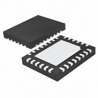
LTC3546IUFD#PBF Linear Technology, LTC3546IUFD#PBF Datasheet - Page 20

LTC3546IUFD#PBF
Manufacturer Part Number
LTC3546IUFD#PBF
Description
IC BUCK SYNC ADJ 1A/2A DL 28QFN
Manufacturer
Linear Technology
Type
Step-Down (Buck)r
Datasheet
1.LTC3546EUFDTRPBF.pdf
(28 pages)
Specifications of LTC3546IUFD#PBF
Internal Switch(s)
Yes
Synchronous Rectifier
Yes
Number Of Outputs
2
Voltage - Output
0.6 ~ 5 V
Current - Output
1A, 2A
Frequency - Switching
2.25MHz, 0.75MHz ~ 4MHz
Voltage - Input
2.25 ~ 5.5 V
Operating Temperature
-40°C ~ 125°C
Mounting Type
Surface Mount
Package / Case
28-QFN
Dc To Dc Converter Type
Step Down
Pin Count
28
Input Voltage
5.5V
Output Voltage
0.6 to 5V
Switching Freq
750 TO 4000/2900KHz
Output Current
2A
Efficiency
96%
Package Type
QFN EP
Output Type
Adjustable
Switching Regulator
Yes
Load Regulation
0.2%
Line Regulation
0.2%/V
Mounting
Surface Mount
Input Voltage (min)
2.25V
Operating Temperature Classification
Automotive
Lead Free Status / RoHS Status
Lead free / RoHS Compliant
Power - Output
-
Lead Free Status / Rohs Status
Compliant
Available stocks
Company
Part Number
Manufacturer
Quantity
Price
APPLICATIONS INFORMATION
LTC3546
tors. This mode provides the best low current effi ciency at
the cost of a higher output voltage ripple. When SYNC/MODE
is connected to ground, pulse-skipping operation is selected
for both regulators. This mode provides a lower output volt-
age and current ripple at the cost of low current effi ciency.
Applying V
regulators. This mode creates a fi xed output ripple and is
capable of sinking some current (about 1/2 • ΔI
the switching noise is constant in this mode, it is also the
easiest to fi lter out. During initial start-up, pulse-skipping
mode is forced until the PGOOD pin goes high.
The LTC3546 can also be synchronized to an external
clock signal by the SYNC/MODE pin. An internal phase
locked loop locks to the incoming signal to provide for
180° out-of-phase operation as well as correct slope
compensation. With external synchronization the FREQ
pin is used for externally compensating the internal phase
locked loop. Typical values used for compensation are 200k
and 100pf, as shown in Figure 6. During synchronization,
the regulator operating mode is forced to pulse skipping.
The P-channel switch turn on is synchronized to the rising
edge of the external clock.
When using an external clock, with the PHASE pin low, the
switching of the two channels occur 180° out-of-phase.
Checking Transient Response
The I
to be optimized for a wide range of loads and output
capacitors. The availability of the I
optimization of the control loop behavior but also pro-
vides a DC-coupled and AC fi ltered closed loop response
test point. The DC step, rise time and settling at this test
point truly refl ects the closed loop response. Assuming a
predominantly second order system, phase margin and/or
damping factor can be estimated using the percentage of
overshoot seen at this pin. The bandwidth can also be
20
TH
pin compensation allows the transient response
IN
/2 results in forced continuous mode for both
Figure 6. PLL Compensation
LTC3546
FREQ
3546 F06
200k
100pF
TH
pin not only allows
L
). Since
estimated using the percentage of overshoot seen at this
pin, or by examining the rise time at this pin.
The I
will provide an adequate starting point for most applica-
tions. The series R-C fi lter sets the dominant pole-zero
loop compensation. The values can be modifi ed slightly
(from 0.5 to 2 times their suggested values) to optimize
transient response once the fi nal PC layout is done and
the particular output capacitor type and value have been
determined. The output capacitors need to be selected
because of various types and values determine the loop
feedback factor gain and phase. An output current pulse
of 20% to 100% of full load current having a rise time
of 1μs to 10μs will produce output voltage and I
waveforms that will give a sense of overall loop stability
without breaking the feedback loop.
Switching regulators take several cycles to respond to
a step in load current. When a load step occurs, V
immediately shifts by an amount equal to ΔI
where ESR is the effective series resistance of C
ΔI
ing a feedback error signal used by the regulator to return
V
V
indicate a stability problem.
The initial output voltage step may not be within the band-
width of the feedback loop, so the standard second order
overshoot/DC ratio cannot be used to determine phase
margin. The gain of the loop increases with R
bandwidth of the loop increases with decreasing C
R
the zero frequency will be kept the same, thereby keeping
the phase the same in the most critical frequency range
of the feedback loop. In addition, feedforward capacitors,
C
response, as shown in Figure 9. Capacitor C
phase lead by creating a high frequency zero with R1
which improves the phase margin for the 1A SW1 chan-
nel. Capacitor C
frequency zero with R3 which improves the phase margin
for the 3A SW1D/SW2 channel.
The output voltage settling behavior is related to the stability
of the closed-loop system and will demonstrate the actual
OUT
OUT
FF1
ITH
LOAD
and C
is increased by the same factor that C
TH
can be monitored for overshoot or ringing that would
to its steady-state value. During this recovery time,
external components shown in the Figure 9 circuit
also begins to charge or discharge C
FF2
, can be added to improve the high frequency
FF2
provides phase lead by creating a high
ITH
is decreased,
OUT
FF1
LOAD
ITH
provides
generat-
OUT
and the
• ESR,
TH
ITH
. The
3546fb
OUT
pin
. If


