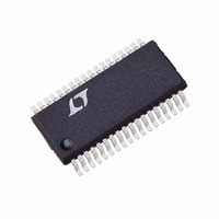
LTC1709EG-85#TRPBF Linear Technology, LTC1709EG-85#TRPBF Datasheet - Page 22

LTC1709EG-85#TRPBF
Manufacturer Part Number
LTC1709EG-85#TRPBF
Description
IC SW REG STEP-DOWN SYNC 36-SSOP
Manufacturer
Linear Technology
Type
Step-Down (Buck)r
Datasheet
1.LTC1709EG-85PBF.pdf
(28 pages)
Specifications of LTC1709EG-85#TRPBF
Internal Switch(s)
No
Synchronous Rectifier
Yes
Number Of Outputs
2
Voltage - Output
1.3 ~ 3.5 V
Current - Output
3A
Voltage - Input
4 ~ 36 V
Operating Temperature
-40°C ~ 85°C
Mounting Type
Surface Mount
Package / Case
36-SSOP
Lead Free Status / RoHS Status
Lead free / RoHS Compliant
Power - Output
-
Frequency - Switching
-
Available stocks
Company
Part Number
Manufacturer
Quantity
Price
APPLICATIO S I FOR ATIO
LTC1709-85
loop and is the filtered and compensated control loop
response. The gain of the loop will be increased by
increasing R
increased by decreasing C
same factor that C
be kept the same, thereby keeping the phase the same in
the most critical frequency range of the feedback loop.
The output voltage settling behavior is related to the
stability of the closed-loop system and will demonstrate
the actual overall supply performance.
Design Example
As a design example, assume V
(max), V
The inductance value is chosen first based on a 30% ripple
current assumption. The highest value of ripple current
occurs at the maximum input voltage. Tie the PLLFLTR pin
to the INTV
inductance for 30% ripple current is:
A 1.5 H inductor will produce 27% ripple current. The
peak inductor current will be the maximum DC value plus
one half the ripple current, or 11.5A. The minimum on-
time occurs at maximum V
The R
maximum current sense voltage specification with some
accomodation for tolerances:
22
R
L
t
ON MIN
SENSE
SENSE
1 35
V
f L
300
.
OUT
OUT
CC
kHz
resistors value can be calculated by using the
= 1.8V, I
H
C
50
11 5
1
V
pin for 300kHz operation. The minimum
V f
and the bandwidth of the loop will be
1 8
OUT
mV
.
IN
.
30
V
A
C
V
V
U
OUT
is decreased, the zero frequency will
IN
MAX
%
0 004
10
5 5
.
= 20A, T
.
U
A
IN
V
C
1 8
. If R
:
IN
.
1
300
= 5V (nominal), V
V
A
= 70 C and f = 300kHz.
1 8
5 5
C
kHz
W
.
.
is increased by the
V
V
11
.
s
U
IN
= 5.5V
The power dissipation on the topside MOSFET can be
easily estimated. Using a Siliconix Si4420DY for example;
R
voltage with T
temperature:
The worst-case power disipated by the synchronous
MOSFET under normal operating conditions at elevated
ambient temperature and estimated 50 C junction tem-
perature rise is:
A short-circuit to ground will result in a folded back current
of about:
The worst-case power disipated by the synchronous
MOSFET under short-circuit conditions at elevated ambi-
ent temperature and estimated 50 C junction temperature
rise is:
which is less than normal, full-load conditions. Inciden-
tally, since the load no longer dissipates power in the
shorted condition, total system power dissipation is de-
creased by over 99%.
DS(ON)
P
P
I
P
SC
MAIN
SYNC
SYNC
= 0.013 , C
0 004
25
.
0 013
1 8
1 29
5 5
300
630
5 5
5 5
.
mV
.
.
.
J
.
.
(estimated) = 110 C at an elevated ambient
V
V
V
V
5 5
5 5
kHz
mW
W
.
.
10 1
V
V
1 8
1 8
2
1
.
.
2
1 7 5 5
RSS
V
V
.
200
0 65
.
10
7
1 5
= 300pF. At maximum input
A
.
ns
0 005 110
A
.
W
.
2
V
2
5 5
1 48 0 013
H
2
.
1 48 0 013
.
10
V
.
A
.
300
.
C
7
A
pF
25
C
170985f


