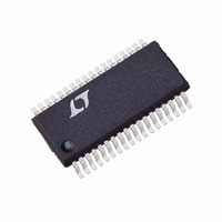
LTC1709EG-85#TRPBF Linear Technology, LTC1709EG-85#TRPBF Datasheet - Page 14

LTC1709EG-85#TRPBF
Manufacturer Part Number
LTC1709EG-85#TRPBF
Description
IC SW REG STEP-DOWN SYNC 36-SSOP
Manufacturer
Linear Technology
Type
Step-Down (Buck)r
Datasheet
1.LTC1709EG-85PBF.pdf
(28 pages)
Specifications of LTC1709EG-85#TRPBF
Internal Switch(s)
No
Synchronous Rectifier
Yes
Number Of Outputs
2
Voltage - Output
1.3 ~ 3.5 V
Current - Output
3A
Voltage - Input
4 ~ 36 V
Operating Temperature
-40°C ~ 85°C
Mounting Type
Surface Mount
Package / Case
36-SSOP
Lead Free Status / RoHS Status
Lead free / RoHS Compliant
Power - Output
-
Frequency - Switching
-
Available stocks
Company
Part Number
Manufacturer
Quantity
Price
APPLICATIO S I FOR ATIO
LTC1709-85
factors for the top and bottom MOSFETs of each output
stage are given by:
The MOSFET power dissipations at maximum output
current are given by:
where is the temperature dependency of R
is a constant inversely related to the gate drive current.
Both MOSFETs have I
equation includes an additional term for transition losses,
which peak at the highest input voltage. For V
high current efficiency generally improves with larger
MOSFETs, while for V
increase to the point that the use of a higher R
with lower C
synchronous MOSFET losses are greatest at high input
voltage when the top switch duty factor is low or during a
short-circuit when the synchronous switch is on close to
100% of the period.
The term (1 + ) is generally given for a MOSFET in the
form of a normalized R
voltage MOSFETs. C
MOSFET characteristics. The constant k = 1.7 can be
used to estimate the contributions of the two terms in the
main switch dissipation equation.
The Schottky diodes, D1 and D2 shown in Figure 1
14
= 0.005/ C can be used as an approximation for low
P
P
Main Switch Duty Cycle
Synchronous Switch Duty Cycle
MAIN
SYNC
k V
V
V
V
OUT
IN
RSS
IN
IN
–
V
2
IN
V
actual provides higher efficiency. The
I
OUT
I
U
MAX
MAX
2
2
IN
2
R losses but the topside N-channel
RSS
> 20V the transition losses rapidly
DS(ON)
I
2
MAX
U
C
2
1
is usually specified in the
RSS
vs temperature curve, but
V
2
V
OUT
IN
R
1
f
DS ON
W
(
R
V
)
DS ON
IN
(
DS(ON)
–
DS(ON)
V
IN
IN
V
)
U
< 20V the
OUT
device
and k
conduct during the dead-time between the conduction of
the two large power MOSFETs. This helps prevent the
body diode of the bottom MOSFET from turning on,
storing charge during the dead-time, and requiring a
reverse recovery period which would reduce efficiency. A
1A to 3A Schottky (depending on output current) diode is
generally a good compromise for both regions of opera-
tion due to the relatively small average current. Larger
diodes result in additional transition losses due to their
larger junction capacitance.
C
In continuous mode, the source current of each top
N-channel MOSFET is a square wave of duty cycle V
V
RMS current must be used. The details of a closed form
equation can be found in Application Note 77. Figure 4
shows the input capacitor ripple current for a 2-phase
configuration with the output voltage fixed and input
voltage varied. The input ripple current is normalized
against the DC output current. The graph can be used in
place of tedious calculations. The minimum input ripple
current can be achieved when the input voltage is twice the
output voltage
In the graph of Figure 4, the 2-phase local maximum input
RMS capacitor currents are reached when:
where k = 1, 2
These worst-case conditions are commonly used for
design because even significant deviations do not offer
much relief. Note that capacitor manufacturer’s ripple
current ratings are often based on only 2000 hours of life.
This makes it advisable to further derate the capacitor, or
to choose a capacitor rated at a higher temperature than
required. Several capacitors may also be paralleled to
meet size or height requirements in the design. Always
consult the capacitor manufacturer if there is any
question.
It is important to note that the efficiency loss is propor-
IN
IN
. A low ESR input capacitor sized for the maximum
V
and C
V
OUT
IN
OUT
2
k
Selection
4
1
170985f
OUT
/


