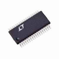
LTC1709EG-85#TRPBF Linear Technology, LTC1709EG-85#TRPBF Datasheet - Page 20

LTC1709EG-85#TRPBF
Manufacturer Part Number
LTC1709EG-85#TRPBF
Description
IC SW REG STEP-DOWN SYNC 36-SSOP
Manufacturer
Linear Technology
Type
Step-Down (Buck)r
Datasheet
1.LTC1709EG-85PBF.pdf
(28 pages)
Specifications of LTC1709EG-85#TRPBF
Internal Switch(s)
No
Synchronous Rectifier
Yes
Number Of Outputs
2
Voltage - Output
1.3 ~ 3.5 V
Current - Output
3A
Voltage - Input
4 ~ 36 V
Operating Temperature
-40°C ~ 85°C
Mounting Type
Surface Mount
Package / Case
36-SSOP
Lead Free Status / RoHS Status
Lead free / RoHS Compliant
Power - Output
-
Frequency - Switching
-
Available stocks
Company
Part Number
Manufacturer
Quantity
Price
APPLICATIO S I FOR ATIO
LTC1709-85
20
FCB Pin Operation
The following table summarizes the possible states avail-
able on the FCB pin:
Table 2
FCB Pin
0.85V < V
V
Voltage Positioning
Voltage positioning can be used to minimize peak-to-peak
output voltage excursion under worst-case transient load-
ing conditions. The open-loop DC gain of the control loop
is reduced depending upon the maximum load step speci-
fications. Voltage positioning can easily be added to the
LTC1709-85 by loading the I
having a Thevenin equivalent voltage source equal to the
midpoint operating voltage of the error amplifier, or 1.2V
(see Figure 7).
The resistive load reduces the DC loop gain while main-
taining the linear control range of the error amplifier. The
worst-case peak-to-peak output voltage deviation due to
transient loading can theoretically be reduced to half or
alternatively the amount of output capacitance can be
reduced for a particular application. A complete explana-
tion is included in Design Solutions 10 or the LTC1736
data sheet. (See www.linear.com)
Figure 7. Active Voltage Positioning Applied to the LTC1709-85
0V to 0.75V
INTVCC
FCB
< V
INTVCC
INTV
CC
R
R
T2
T1
– 2V
U
R
C
C
C
U
Condition
Forced Continuous (Current Reversal
Allowed—Burst Inhibited)
Minimum Peak Current Induces
Burst Mode Operation
No Current Reversal Allowed
Burst Mode Operation Disabled
Constant Frequency Mode Enabled
No Current Reversal Allowed
No Minimum Peak Current
TH
I
TH
pin with a resistive divider
LTC1709-85
W
170985 F08
U
Efficiency Considerations
The percent efficiency of a switching regulator is equal to
the output power divided by the input power times 100%.
It is often useful to analyze individual losses to determine
what is limiting the efficiency and which change would
produce the most improvement. Percent efficiency can be
expressed as:
where L1, L2, etc. are the individual losses as a percentage
of input power.
Although all dissipative elements in the circuit produce
losses, four main sources usually account for most of the
losses in LTC1709-85 circuits: 1) I
MOSFET transition losses, 3) INTV
and 4) LTC1709-85 V
differential amplifier output).
1) I
fuse (if used), MOSFET, inductor, current sense resistor,
and input and output capacitor ESR. In continuous mode
the average output current flows through L and R
but is “chopped” between the topside MOSFET and the
synchronous MOSFET. If the two MOSFETs have approxi-
mately the same R
MOSFET can simply be summed with the resistances of L,
R
R
total resistance is 25m . This results in losses ranging
from 2% to 8% as the output current increases from 3A to
15A per output stage for a 5V output, or a 3% to 12% loss
per output stage for a 3.3V output. Efficiency varies as the
inverse square of V
and output power level. The combined effects of increas-
ingly lower output voltages and higher currents required
by high performance digital systems is not doubling but
quadrupling the importance of loss terms in the switching
regulator system!
2) Transition losses apply only to the topside MOSFET(s),
and are significant only when operating at high input
voltages (typically 12V or greater). Transition losses can
be estimated from:
SENSE
DS(ON)
Transition Loss = (1.7) V
%Efficiency = 100% – (L1 + L2 + L3 + ...)
2
R losses are predicted from the DC resistances of the
and ESR to obtain I
= 10m , R
L
OUT
= 10m , and R
DS(ON)
IN
for the same external components
current (including loading on the
2
, then the resistance of one
IN
R losses. For example, if each
2
I
O(MAX)
2
SENSE
R losses, 2) Topside
CC
C
regulator current
RSS
= 5m , then the
f
SENSE
170985f
,


