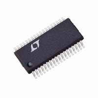
LTC3731HG#PBF Linear Technology, LTC3731HG#PBF Datasheet - Page 14

LTC3731HG#PBF
Manufacturer Part Number
LTC3731HG#PBF
Description
IC SW REG CTRLR SYNC BUCK 36SSOP
Manufacturer
Linear Technology
Series
PolyPhase®r
Type
Step-Down (Buck)r
Datasheet
1.LTC3731HG.pdf
(34 pages)
Specifications of LTC3731HG#PBF
Internal Switch(s)
No
Synchronous Rectifier
Yes
Number Of Outputs
1
Voltage - Output
0.6 ~ 6 V
Frequency - Switching
225kHz ~ 680kHz
Voltage - Input
4 ~ 36 V
Operating Temperature
-40°C ~ 140°C
Mounting Type
Surface Mount
Package / Case
36-SSOP
Primary Input Voltage
7V
No. Of Outputs
1
Output Voltage
32V
Output Current
5A
No. Of Pins
36
Operating Temperature Range
0°C To +70°C
Msl
MSL 1 - Unlimited
Rohs Compliant
Yes
Lead Free Status / RoHS Status
Lead free / RoHS Compliant
Current - Output
-
Power - Output
-
Available stocks
Company
Part Number
Manufacturer
Quantity
Price
LTC3731H
applicaTions inForMaTion
MOSFET in applications that have an output voltage that
is less than 1/3 of the input voltage. In applications where
V
less important for overall efficiency than its input capaci-
tance at operating frequencies above 300kHz. MOSFET
manufacturers have designed special purpose devices that
provide reasonably low on-resistance with significantly
reduced input capacitance for the main switch application
in switching regulators.
The peak-to-peak MOSFET gate drive levels are set by the
voltage, V
MOSFETs in most applications. Pay close attention to the
BV
logic-level MOSFETs are limited to 30V or less.
Selection criteria for the power MOSFETs include the
on-resistance R
and maximum output current.
MOSFET input capacitance is a combination of sev-
eral components but can be taken from the typical “gate
charge” curve included on most data sheets (Figure 5).
The curve is generated by forcing a constant input cur-
rent into the gate of a common source, current source
loaded stage and then plotting the gate voltage versus
time. The initial slope is the effect of the gate-to-source
and the gate-to-drain capacitance. The flat portion of the
curve is the result of the Miller multiplication effect of the
drain-to-gate capacitance as the drain drops the voltage
across the current source load. The upper sloping line is
due to the drain-to-gate accumulation capacitance and
the gate-to-source capacitance. The Miller charge (the
increase in coulombs on the horizontal axis from a to b
while the curve is flat) is specified for a given V
IN
DSS
>> V
V
GS
specification for the MOSFETs as well; many of the
OUT
CC
C
MILLER
, the top MOSFETs’ on-resistance is normally
Figure 5. Gate Charge Characteristic
, requiring the use of logic-level threshold
a
MILLER EFFECT
= (Q
DS(ON)
Q
IN
B
– Q
A
, input capacitance, input voltage
)/V
b
DS
V
+
GS
–
V
+
–
3731H F05
V
DS
DS
V
IN
drain
voltage, but can be adjusted for different V
multiplying by the ratio of the application V
specified V
is to take the change in gate charge from points a and b
on a manufacturers data sheet and divide by the stated
V
lection criteria for determining the transition loss term in
the top MOSFET but is not directly specified on MOSFET
data sheets. C
definitions of these parameters are not included.
When the controller is operating in continuous mode
the duty cycles for the top and bottom MOSFETs are
given by:
The power dissipation for the main and synchronous
MOSFETs at maximum output current are given by:
where N is the number of output stages, d is the tem-
perature dependency of R
driver resistance (approximately 2Ω at V
is the drain potential and the change in drain potential in
the particular application. V
fied typical gate threshold voltage specified in the power
MOSFET data sheet at the specified drain current. C
is the calculated capacitance using the gate charge curve
from the MOSFET data sheet and the technique described
above.
DS
P
Main Switch Duty Cycle
Synchronous Switch Duty Cycle
P
SYNC
MAIN
voltage specified. C
=
=
DS
V
V
V
V
IN
IN
OUT
V
values. A way to estimate the C
IN
RSS
CC
2
–
V
I
IN
MAX
2
–
V
and C
N
OUT
I
1
V
MAX
N
TH IL
(
R
( )
MILLER
DR
OS
I
MAX
2
DS(ON)
N
(
)(
+
TH(IL)
are specified sometimes but
1
=
C
+
V
V
MILLER
TH IL
is the most important se-
d
2
V
OUT
, R
1
(
IN
)
( )
1
is the data sheet speci-
R
+
DR
DS ON
d
=
)
(
( )
)
is the effective top
f
•
R
GS
V
)
DS ON
IN
= V
DS
DS
+
(
–
V
to the curve
MILLER
MILLER
voltages by
IN
V
)
OUT
MILLER
), V
3731Hfb
term
IN


