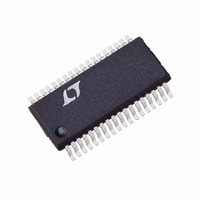
LTC3731HG#PBF Linear Technology, LTC3731HG#PBF Datasheet - Page 10

LTC3731HG#PBF
Manufacturer Part Number
LTC3731HG#PBF
Description
IC SW REG CTRLR SYNC BUCK 36SSOP
Manufacturer
Linear Technology
Series
PolyPhase®r
Type
Step-Down (Buck)r
Datasheet
1.LTC3731HG.pdf
(34 pages)
Specifications of LTC3731HG#PBF
Internal Switch(s)
No
Synchronous Rectifier
Yes
Number Of Outputs
1
Voltage - Output
0.6 ~ 6 V
Frequency - Switching
225kHz ~ 680kHz
Voltage - Input
4 ~ 36 V
Operating Temperature
-40°C ~ 140°C
Mounting Type
Surface Mount
Package / Case
36-SSOP
Primary Input Voltage
7V
No. Of Outputs
1
Output Voltage
32V
Output Current
5A
No. Of Pins
36
Operating Temperature Range
0°C To +70°C
Msl
MSL 1 - Unlimited
Rohs Compliant
Yes
Lead Free Status / RoHS Status
Lead free / RoHS Compliant
Current - Output
-
Power - Output
-
Available stocks
Company
Part Number
Manufacturer
Quantity
Price
operaTion
LTC3731H
Main Control Loop
The IC uses a constant frequency, current mode step-down
architecture. During normal operation, each top MOSFET
is turned on each cycle when the oscillator sets the RS
latch, and turned off when the main current comparator,
I
which I
on the I
EA. The EAIN pin receives a portion of output voltage
feedback signal through the external resistive divider and
is compared to the internal reference voltage. When the
load current increases, it causes a slight decrease in the
EAIN pin voltage relative to the 0.6V reference, which in
turn causes the I
average current matches one third of the new load current
(assuming all three current sensing resistors are equal).
In Burst Mode operation and stage shedding mode, after
each top MOSFET has turned off, the bottom MOSFET is
turned on until either the inductor current starts to reverse,
as indicated by current comparator I
of the next cycle.
The top MOSFET drivers are biased from floating bootstrap
capacitor C
external Schottky diode when the top FET is turned off.
When V
the loop may enter dropout and attempt to turn on the
top MOSFET continuously. The dropout detector counts
the number of oscillator cycles that the bottom MOSFET
remains off and periodically forces a brief on period to
allow C
The main control loop is shut down by pulling the RUN/SS
pin low. Releasing RUN/SS allows an internal 1.5µA
current source to charge soft-start capacitor C
C
the internally buffered I
to ramp as the voltage on C
“soft-start” clamping prevents abrupt current from being
drawn from the input power source. When the RUN/SS
pin is low, all functions are kept in a controlled state.
The RUN/SS pin is pulled low when the supply input
voltage is below 4V, when the undervoltage lockout pin
(UVADJ) is below 1.2V, or when the IC die temperature
rises above 160°C.
0
1
SS
, resets each RS latch. The peak inductor current at
reaches 1.5V, the main control loop is enabled and
B
1
TH
IN
resets the RS latch is controlled by the voltage
to recharge.
decreases to a voltage close to V
pin, which is the output of the error amplifier
B
, which is normally recharged through an
TH
voltage to increase until each inductor’s
(Refer to Functional Diagram)
TH
voltage is clamped but allowed
SS
continues to ramp. This
2
, or the beginning
OUT
, however,
SS
. When
Low Current Operation
The FCB pin is a logic input to select between three modes
of operation.
A) Burst Mode Operation
When the FCB pin voltage is below 0.6V, the controller
performs as a continuous, PWM current mode synchro-
nous switching regulator. The top and bottom MOSFETs
are alternately turned on to maintain the output voltage
independent of direction of inductor current. When the
FCB pin is below V
controller performs as a Burst Mode switching regulator.
Burst Mode operation sets a minimum output current
level before turning off the top switch and turns off the
synchronous MOSFET(s) when the inductor current goes
negative. This combination of requirements will, at low
current, force the I
will temporarily shut off both output MOSFETs until the
output voltage drops slightly. There is a burst compara-
tor having 60mV of hysteresis tied to the I
hysteresis results in output signals to the MOSFETs that
turn them on for several cycles, followed by a variable
“sleep” interval depending upon the load current. The
resultant output voltage ripple is held to a very small
value by having the hysteretic comparator after the error
amplifier gain block.
B) Stage Shedding Operation
When the FCB pin is tied to the V
tion is disabled and the forced minimum inductor current
requirement is removed. This provides constant frequency,
discontinuous current operation over the widest possible
output current range. At approximately 10% of maximum
designed load current, the second and third output stages
are shut off and the phase 1 controller alone is active in
discontinuous current mode. This “stage shedding” opti-
mizes efficiency by eliminating the gate charging losses and
switching losses of the other two output stages. Additional
cycles will be skipped when the output load current drops
below 1% of maximum designed load current in order to
maintain the output voltage. This stage shedding operation
is not as efficient as Burst Mode operation at very light
loads, but does provide lower noise, constant frequency
operating mode down to very light load conditions.
TH
CC
pin below a voltage threshold that
– 1.5V but greater than 0.6V, the
CC
pin, Burst Mode opera-
TH
pin. This
3731Hfb


