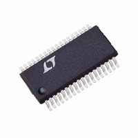
LTC3731HG#PBF Linear Technology, LTC3731HG#PBF Datasheet - Page 13

LTC3731HG#PBF
Manufacturer Part Number
LTC3731HG#PBF
Description
IC SW REG CTRLR SYNC BUCK 36SSOP
Manufacturer
Linear Technology
Series
PolyPhase®r
Type
Step-Down (Buck)r
Datasheet
1.LTC3731HG.pdf
(34 pages)
Specifications of LTC3731HG#PBF
Internal Switch(s)
No
Synchronous Rectifier
Yes
Number Of Outputs
1
Voltage - Output
0.6 ~ 6 V
Frequency - Switching
225kHz ~ 680kHz
Voltage - Input
4 ~ 36 V
Operating Temperature
-40°C ~ 140°C
Mounting Type
Surface Mount
Package / Case
36-SSOP
Primary Input Voltage
7V
No. Of Outputs
1
Output Voltage
32V
Output Current
5A
No. Of Pins
36
Operating Temperature Range
0°C To +70°C
Msl
MSL 1 - Unlimited
Rohs Compliant
Yes
Lead Free Status / RoHS Status
Lead free / RoHS Compliant
Current - Output
-
Power - Output
-
Available stocks
Company
Part Number
Manufacturer
Quantity
Price
applicaTions inForMaTion
In a PolyPhase converter, the net ripple current seen by
the output capacitor is much smaller than the individual
inductor ripple currents due to the ripple cancellation. The
details on how to calculate the net output ripple current
can be found in Application Note 77.
Figure 4 shows the net ripple current seen by the output
capacitors for the different phase configurations. The
output ripple current is plotted for a fixed output voltage
as the duty factor is varied between 10% and 90% on the
x-axis. The output ripple current is normalized against the
inductor ripple current at zero duty factor. The graph can be
used in place of tedious calculations. As shown in Figure
4, the zero output ripple current is obtained when:
So the number of phases used can be selected to minimize
the output ripple current and therefore the output ripple
voltage at the given input and output voltages. In appli-
cations having a highly varying input voltage, additional
phases will produce the best results.
Accepting larger values of ∆I
ductances but can result in higher output voltage ripple.
A reasonable starting point for setting ripple current is
∆I
I
∆I
inductor ripple currents are constant determined by the
input and output voltages, and the inductance.
Inductor Core Selection
Once the value for L1 to L3 is determined, the type of induc-
tor must be selected. High efficiency converters generally
cannot afford the core loss found in low cost powdered iron
cores, forcing the use of ferrite, molypermalloy or Kool Mµ
cores. Actual core loss is independent of core size for a
fixed inductor value, but it is very dependent on inductance
selected. As inductance increases, core losses go down.
Unfortunately, increased inductance requires more turns
of wire and therefore copper losses will increase.
OUT
L
L
V
= 0.4(I
occurs at the maximum input voltage. The individual
V
OUT
is the total load current. Remember, the maximum
IN
=
OUT
N
k
)/N, where N is the number of channels and
where k
= 1 2
, , ..., –
L
allows the use of low in-
N
1
Ferrite designs have very low core loss and are preferred
at high switching frequencies, so design goals cancon-
centrate on copper loss and preventing saturation. Ferrite
core material saturates “hard,” which means that induc-
tance collapses abruptly when the peak design current is
exceeded. This results in an abrupt increase in inductor
ripple current and consequent output voltage ripple. Do
not allow the core to saturate!
Molypermalloy (from Magnetics, Inc.) is a very good, low
loss core material for toroids, but it is more expensive
than ferrite. A reasonable compromise from the same
manufacturer is Kool Mµ. Toroids are very space effi-
cient, especially when you can use several layers of wire.
Because they lack a bobbin, mounting is more difficult.
However, designs for surface mount are available which
do not increase the height significantly.
Power MOSFET and D1, D2, D3 Selection
At least two external power MOSFETs must be selected for
each of the three output sections: One N-channel MOSFET
for the top (main) switch and one or more N-channel
MOSFET(s) for the bottom (synchronous) switch. The
number, type and on-resistance of all MOSFETs selected
take into account the voltage step-down ratio as well as
the actual position (main or synchronous) in which the
MOSFET will be used. A much smaller and much lower
input capacitance MOSFET should be used for the top
Figure 4. Normalized Peak Output Current
vs Duty Factor [I
1.0
0.9
0.8
0.7
0.6
0.5
0.4
0.3
0.2
0.1
0
0.1
0.2
0.3
DUTY FACTOR (V
RMS
0.4
0.5
= 0.3(I
OUT
0.6
/V
O(P-P)
IN
0.7
LTC3731H
1-PHASE
2-PHASE
3-PHASE
4-PHASE
6-PHASE
12-PHASE
)
]
0.8
3731H F04
0.9
3731Hfb


